MINAFAB Processiong equipments

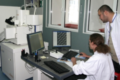
Electron beam lithography and nanoengineering workstation- Raith e_Line from RAITH GmbH

Technical characteristics:

Ultra high resolution electron beam lithography and nano engineering workstation Raith e_Line is a versatile electron beam lithography system having complied with the specific requirements of interdisciplinary research.
Selected options for nanomanipu-lation, EBID and EBIE expand this system to a nano-engineering workstation.
The state-of-the-art e_LiNE electron column matches perfectly with a number of key applications in: nanoelectroniccs, photonic crystals (PCs),  Difractve Optic Elements (DOE),  CNTs  interconections, nanodevices and nanosystems for fundamental research and bio applications.

Basic hardware features:

  • Thermal assisted field emission gun;
  • Cross-over free column with highest beam current density at 2 nm spot size;
  • Laser interferometer stage with 100 mm by 100 mm travel range and 2 nm resolution achieved by closed-loop piezo-positioning;
  • 10 MHZ DSP-controlled digital pattern generator;
  • Optional gas injection system, nanomanipulators, EDX, optical microscope, loadlock, rotation and tilt module, FBMS mode exposure;
  • Minimum line width < 20 nm;  Stitching accuracy 40 nm;  Overlay accuracy 40 nm;

**********************

Nano engineering options:

  • Gas injector unit with up to five capillaries;
  • Nano prober arrangement with up to four needles;
  • Retractable x-ray analysis unit;
  • Optical microscope;
  • Height sensor;
  • Load lock;
  • Rotation tilt module for SEM inspection;

**********************

Applications:

  • Nano lithography with sub 20 nm resolution;
  •  High speed devices e.g. HEMT;
  • CMOS process and device developments;
  • Resist less lithography;
  • E-beam induced deposition and etching;
  • Imprint template fabrication;
  • Nano probing and electrical measurements;
  • Nano and pattern placement metrology;
  • Fabrication of photonic crystals;

Photonic cristalsin PMMA on silicon for near IR application

  • Gratings, DFB lasers, SAW devices;

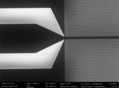
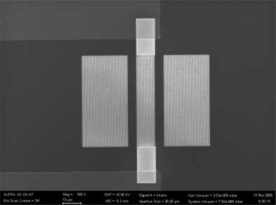
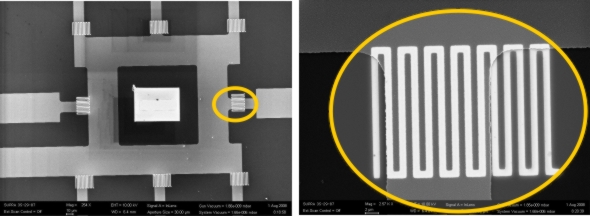
SAW device for microwave applications obtained using mix and match
lithography (EBL and optical lithography)

  • Three-dimensional structures;

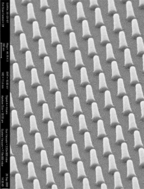
Diffractive Optical Element (DOE) for photonics applications

  • Optical devices, holograms, micro lenses;


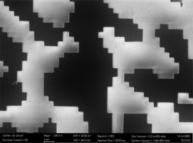
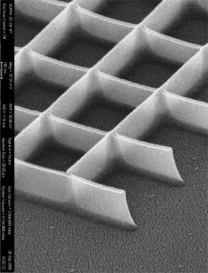
High aspect ratio (12:1) structures in PMMA applications in nanotechnology.
Left: crosslines; Rigth nanopilars.

  • High resolution SEM inspection;

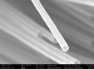
High resolution CNTs imaging.

******************************************************************
Results:
mix-and-match lithography for biomedical applications: optical lithography (left),
combined with EBL (right)

Partneship:

 CATHERINE- Carbon nAnotube Technology for High-speed nExt-geneRation nano-InterconNEcts, STREP, FP7-ICT, 2008-2011


Application scientist: Phys. Adrian Dinescu, [email protected]


HOME

top of page

Last update: March 05, 2012