

| MINAFAB | Characterization equipments |
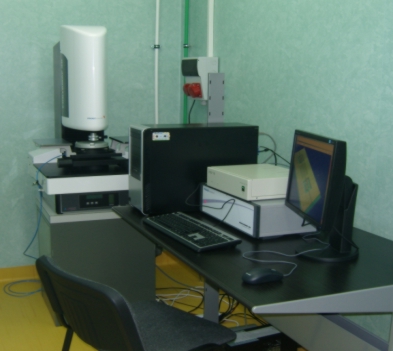
White Light Interferometer
Technical characteristics: Caracteristics: manual translation stage 100x100 mm range, 20μm resolution; optical head vertical range 150 mm; nanometric objective translation unit; capacitive sensor closed loop control, 500 μm range; white light and Monochromatic light source; automatic switching, software control; antivibration feet; field of view 126 x 96 μm up to 2.5 x 1.9 mm depending on objective (without zoom); white light profilometry, 3 nm rms z resolution; monochromatic light profilometry, 0.1 nm rms z resolution; automatic step height and roughness measurement; semi-automatic focus detection; results exploitation (heights, roughness, dimensions, field stitching, filtering, 3D view, bump size, height, roughness measurements); motorized x0.35 to 1.6 zoom; out of plane measurements (by stroboscopic interferometry within range 100Hz - 2MHz and by time averaged operation without frequency limitations); synthetized function generator: 2 channels controlled by software (one channel for stroboscopic illumination, the other one for MEMS AC voltage supply); high voltage module (amplitude up to 200V; offset up to 200V; 1% resolution; sinusoidal and square signal; power 20W; current output max 100 mA); multi-reflectivity (5%,25%,50%,85%) objectives (x2.5, x5, x20); motorised XY stage; active vibration isolation stage. |
 |
Description The white light interferometer perform optical, non-contact profiling of rough surfaces, that uses interferometric techniques as well as digital signal processing algorithms to produce fast, accurate, repeatable two and three-dimensional surface profile measurements. The method of determining surface height is based on white light as the source in an interferometer, and measurements of the fringe modulation degree, or coherence, instead of the phase of interference fringes. The white light interferometric profilometer uses the measurement of surface height through vertical scanning of the reference arm of the interferometer, and calculate the relative modulation of the intensity signal as a function of vertical position. The equipment present sub-nanometer vertical resolution (down to 0.1 nm) at all magnifications, non-contact measurements allowing accurate and repeatable results, all axes motorization enabling automatic stitching of multiples fields of view, sub-nanometric roughness measurements, reflectivity 1% to 100%, ability to measure transparent films and require no sample preparation. ********************** |
|
Applications:
**************************************************************************************** |
|
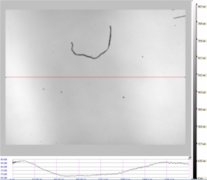
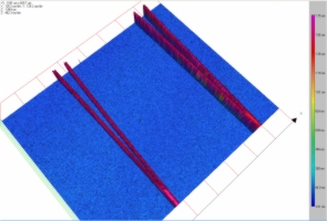
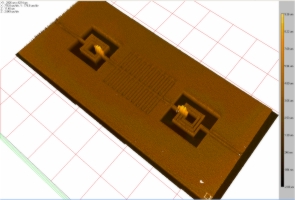
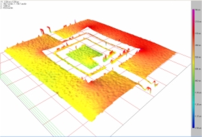
| Results: | |||||||||
|
|||||||||
Partneship:
******************************************************************
|
|||||||||
Application scientist: dr. phys. Alina Cismaru, alina.cismaru@imt.ro |
|||||||||
|
|
Last update: March 5 2012 |