Electromagnetic simulations and design of 77 GHz antenna in LTCC technology.
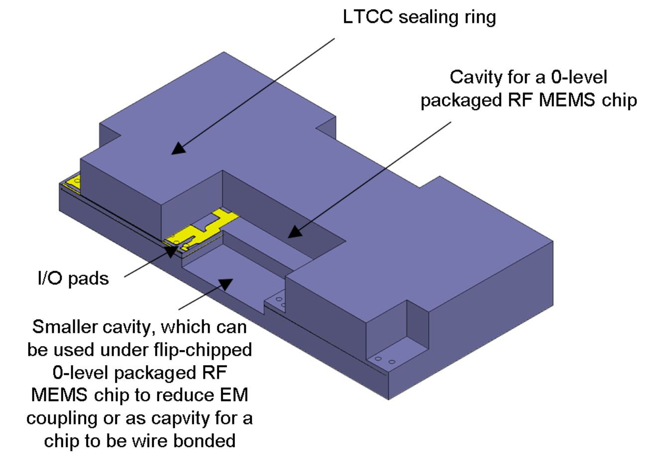
Fig.1. Cross section of a LTCC structure with isolation ring (lay 14), metallisations (in yellow on lay 6), small cavity on lay 3.
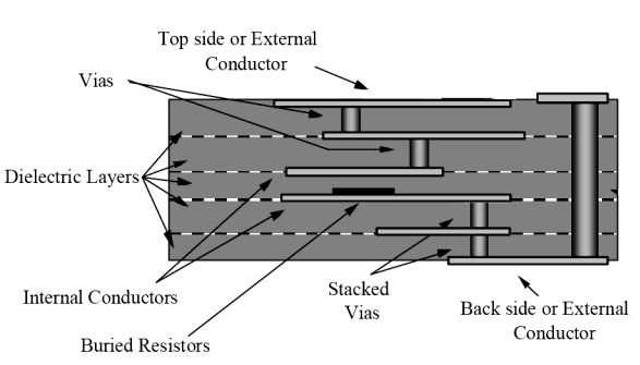
Fig.2. Cross section of a LTCC structure
Antena microstrip patch (MPA)
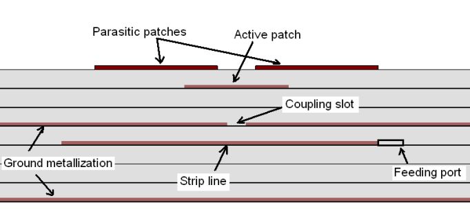
Fig.3. Cross section of a antenna structure in LTCC technology
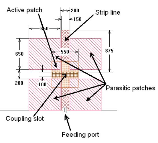
Fig.4. 77 GHz Optimised antenna layout
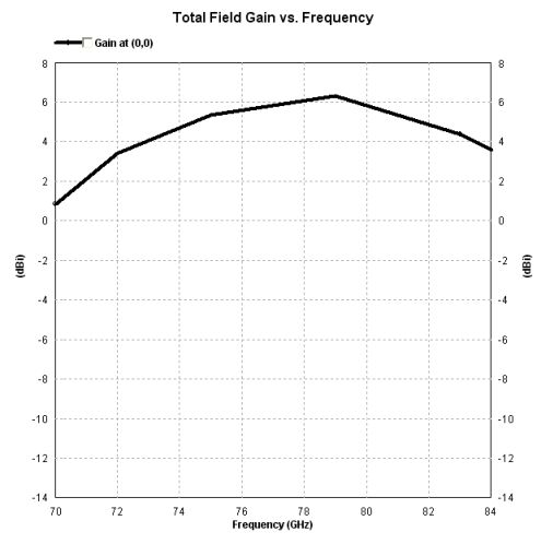
Fig.5. Simulations result for77 GHz antenna gain
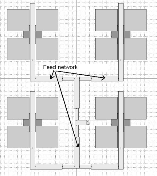
Fig 6. Lay-out of the 2x2 antennas array
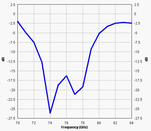
Fig.7.Simulations results for Reflexive losses of 2x2 antennas array
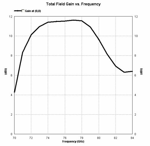
Fig.8 Simulations results for the gain of 2x2 antennas array
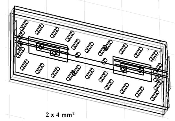
Fig.9. 3-D image of 2 vertical connections through SL-stripline
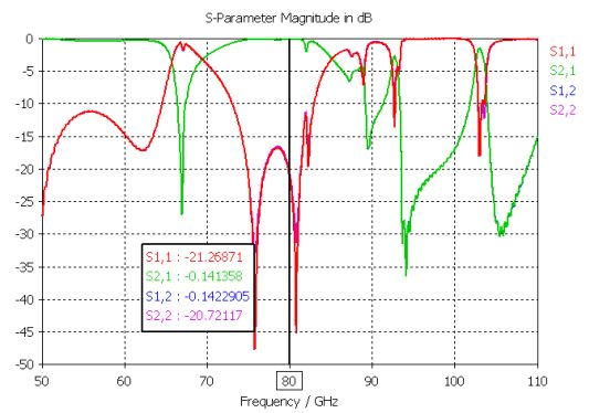
Fig.10. Simulations results of S parametres for vertical connections through SL-stripline
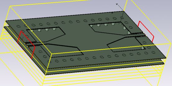
Fig.11. 3D image of two CPW-SIW transitions connected by SIW
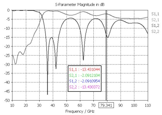
Fig.12.S parameters- Simulations results for two CPW-SIW transitions
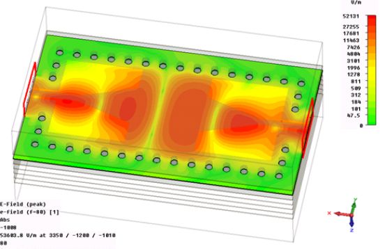
Fig.13. E-field distribution for two CPW-SIW transitions
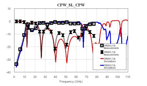
Fig. 14. Measurements and simulations resuts for S parameters of CPW_SL_CPW
Design and optimisation for a 77 GHz receiver in LTCC technology
The receiver module is based on flip-cip Schottky diode on GaAs DMK 2790 Skyworks Solutions Inc., with the characteristics: RS = 4 W, CT=0.05 pF (capacitance Cp = 0.02 pF), ideality factor n = 1.05, saturation current IS = 0.5 pA.
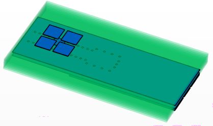
Fig.15. 3D image of receiver structure (antenna area)
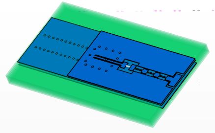
Fig.15. 3D image of receiver structure (Schottky diode area)
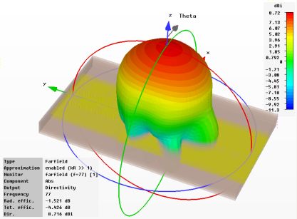
Fig 17. 3D simulation for pattern radiation of 77 GHz antenna

Fig.18. Photo image of receiver structure (antenna contacts area) in LTCC technology
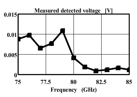
Fig.19. Measurements of detected voltage at diode contacts versus frequency (DC current is 45 μA)
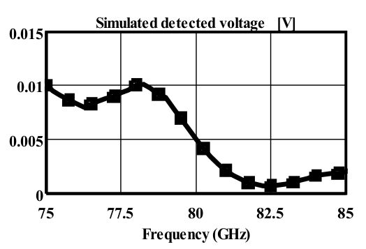
Fig.20. Simulations results for detected voltage at diode contacts versus frequency (DC current is 45 μA)
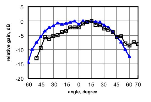
Fig.21. Radiation pattern in 2D measured at 77 GHz (triangles –plane H)
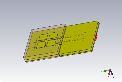
Fig.22. Optimised antenna element for 77 GHz
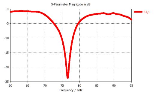
Fig. 23. S11 parameter (reflexion losses) for the 77 GHz Optimised antenna element
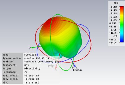
Fig.24. Radiation pattern for the optimised antenna element
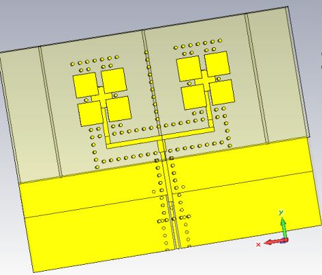
Fig.25. 2x1 antennas array for 77 GHz
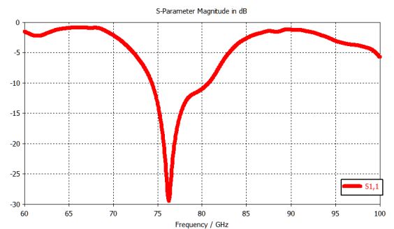
Fig.26. reflexion losses for 77GHz 2x1 antennas array
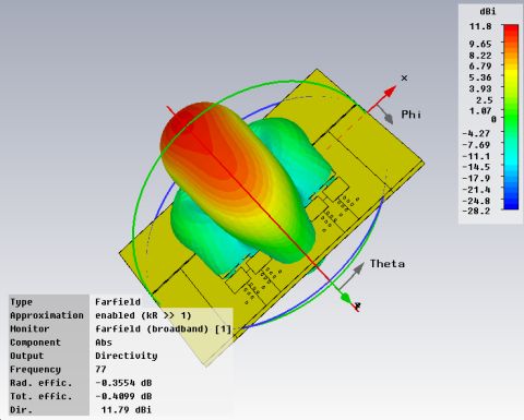
Fig.27. Radiation pattern for2x1 antennas array at 77 GHz
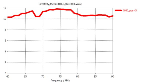
Fig.28. Wide band directivity of main radiation direction of 2x1 antennas array
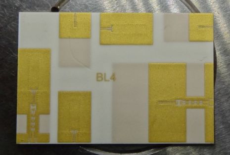
Fig.29. Image of structures in LTCC technology

Fig.30. Experimental set-up of “on wafer” measurements for 77GHz antennas structures
2x1 antennas array module optimised at 77GHz – experimental results
“on wafer” measurements for 77GHz antennas structures are presented in fig 31 . One can observes a good agreement with the simulations results as well as better performances for the band width, extended to 74-88 GHz
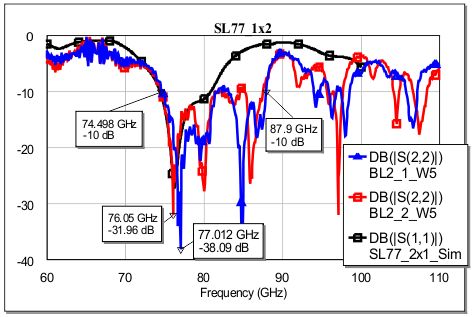
Fig.31. Experimental results in comparaison with simulations results
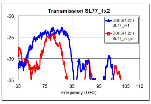
Fig.32. S21 measurements for the 2x1 antenna array and the antenna element