Main results obtained in 2012
The material properties can be measured in free space through methods of reflection or transmission, with a focalized or unfocalized microwave beam. The first measurements were performed with a measurement setup calibrated for on wafer measurements with coplanar waveguide standards (no rectangular waveguide or free space calibration could be performed at the time). The horn antennas used in the experiment, radiate an unfocalized microwave beam. The tests were performed with the setup shown in Fig. 1 (a) for reflection measurements and Fig. 1 (b) for transmission measurements. W-band absorbent materials were acquired and a Thru (Fig.2 (a)) – Reflect (Fig.2 (b)) – Match (Fig.2 (c)) calibration standard is currently being developed.
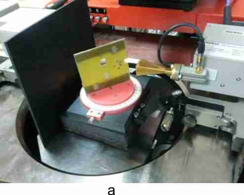
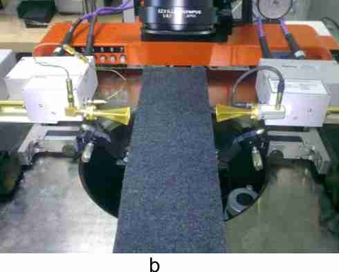
Fig. 1. (a) Material parameters measurement system through reflection; (b) Material parameters measurement system through transmission
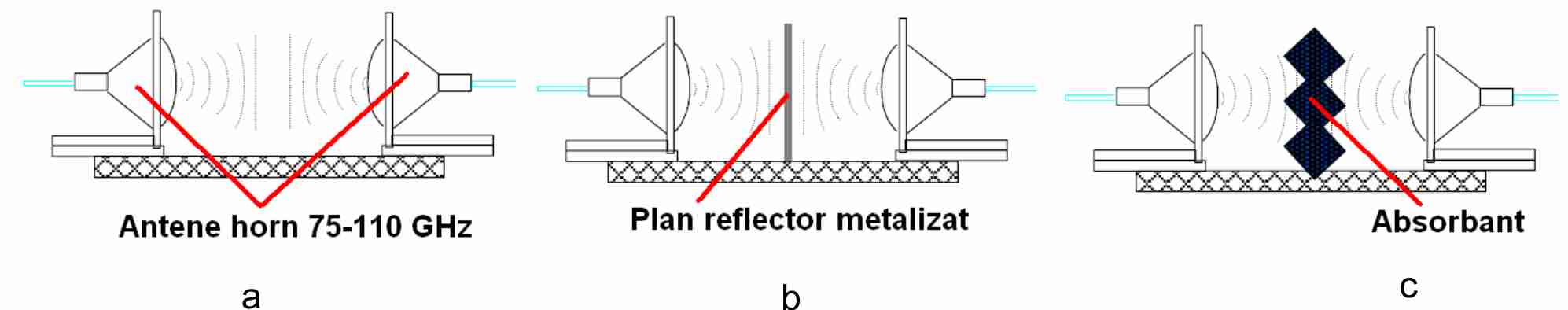
Fig. 2. Calibration standard for free space material parameter measurements (a) Thru(b) Reflect (c) Match
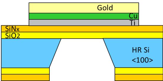
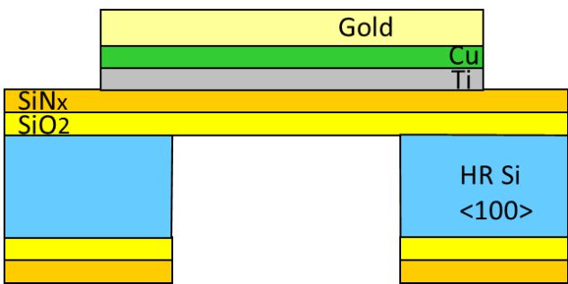
High resistivity silicon micromachining technologies for the fabrication of thin dielectric membranes were developed. For the dielectric layers, two materials which are easily obtained in the silicon technology processes were chosen: thermal silicon dioxide and silicon nitride. The thickness of each layer is selected so as to ensure the stress compensation and a good mechanical stability and planarity for the metallic layers. There are two basic silicon micromachining technologies: anisotropic wet etching (Fig. 3 (a)) and deep reactive ion etching (Fig. 3 (b)). The experimental results for this stage are presented in Fig. 4 (there are no metallic layers on the dielectric membranes). A good fabrication yield can be noticed.
 b
b
 a
a
Fig.3 (a) silicon anisotropic wet etching (b) silicon deep reactive ion etching;
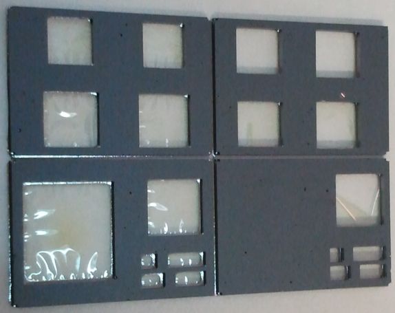
Fig.4 Deep reactive ion etching of silicon wafer (back side view)
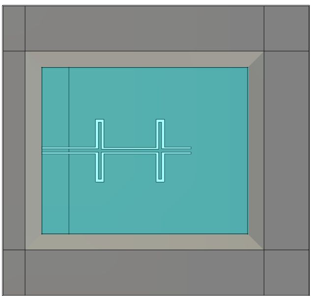
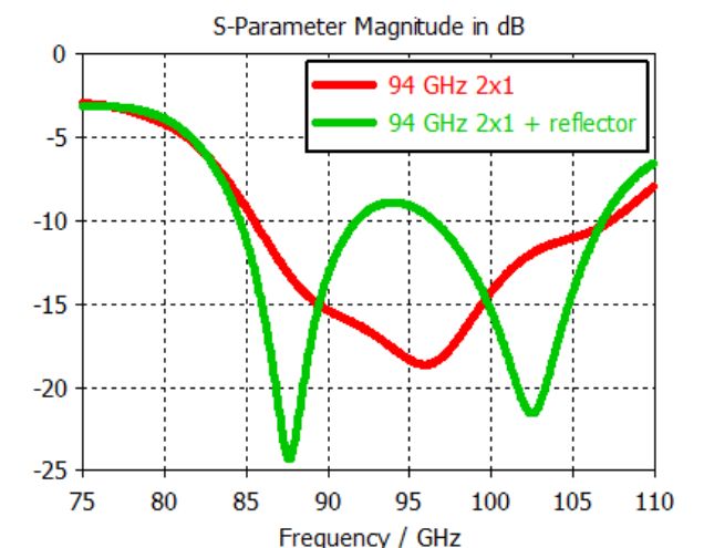
Double folded slot antenna arrays with 2 and 3 radiating elements were modeled and designed, for the 94 GHz and 140 GHz operating frequencies. Fig. 5 (a) shows the general layout of the 2x1 antenna array, while Fig. 5 (b) shows the matching for the 94 GHz operating frequency design, without and with an additional reflector element.
 a
a
 b
b
Fig 5. (a) Layout of the 2x1 antenna array; (b) reflection parameter for the 2x1 antenna array at 94 GHz;
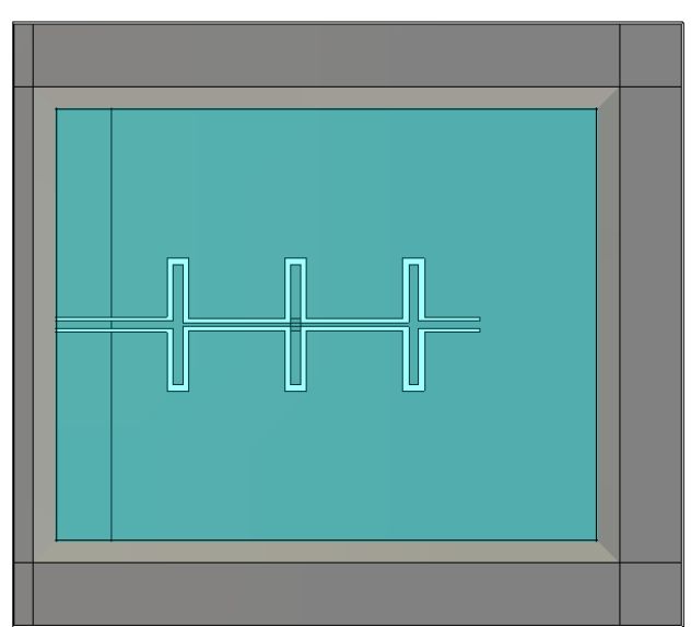
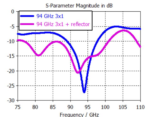
Fig. 6 (a) shows the general layout of the 3x1 antenna array, while Fig. 6 (b) shows the matching for the 94 GHz operating frequency design, without and with an additional reflector element.
 a
a
 b
b
Fig 6. (a) Layout of the 3x1 antenna array; (b) reflection parameter for the 3x1 antenna array at 94 GHz;
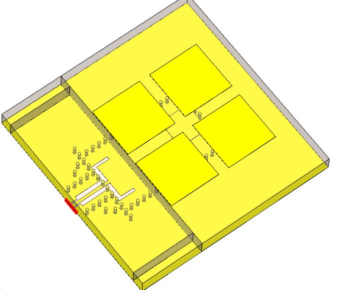
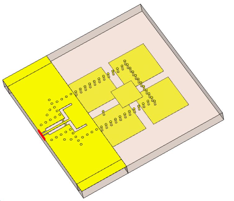
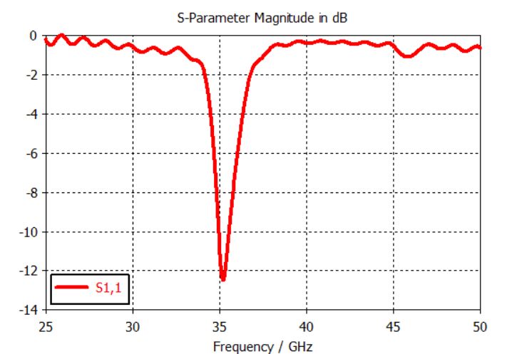
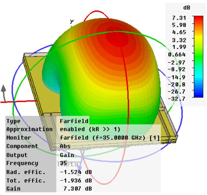
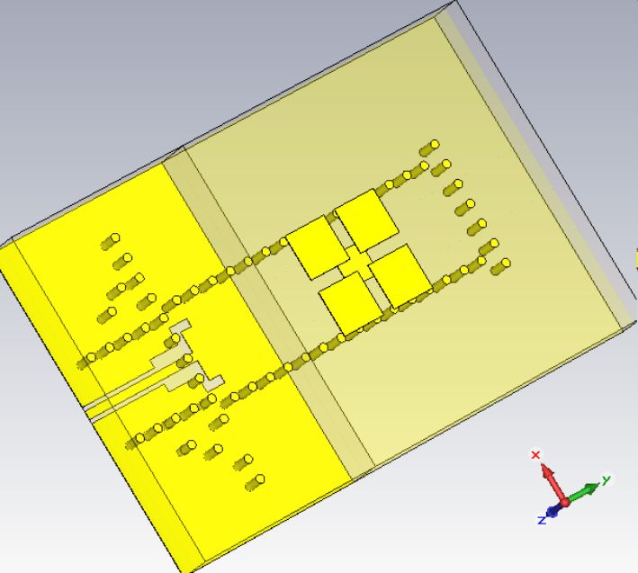
Substrate integrated waveguide (SIW) antenna structures were investigated. The multilayer Low-Temperature Cofired Ceramic (LTCC) technology was considered for fabrication. Fig. 7 (a) and (b) show 3D views of the 35 GHz antenna structure, designed for 6 dielectric layers. Fig. 7 (c) shows the reflection losses at the feed port, while Fig. 7 (d) shows the 3D radiation characteristic.
 a
a
 b
b
 c
c
 d
d
Fig.7 35 GHz SIW LTCC antenna structure: (a) 3D front side view; (b) 3D back side view; (c) |S11| parameter; (d) 3D radiation characteristic
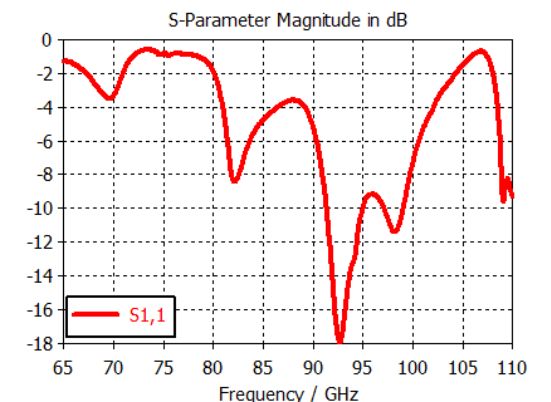
For the 94 GHz operating frequency, the 3D front side view is presented in Fig. 8 (a). The reflection losses (Fig.8 (b)) show a 10 % fractional operating band, with a maximum directivity of 7dBi (Fig. 8 (c)).
 a
a
 b
b
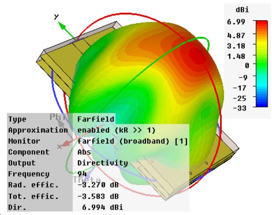 c
c
Fig. 8 94 GHz SIW LTCC antenna structure: (a) 3D front side view; (b) |S11| parameter; (c) 3D radiation characteristic