Main results obtained in 2015
1. Introduction
The system integration of the millimeter wave imaging sensor is reported in this phase. The various component blocks investigated in the previous phases are hybrid integrated in a single system. Integration technologies based on conductive epoxy and thermocompression wire bonding are investigated. The entire frontend is placed on a Printed Circuit Board and connected to coaxial connectors that ensure the interface with the measurement system.
2. System design
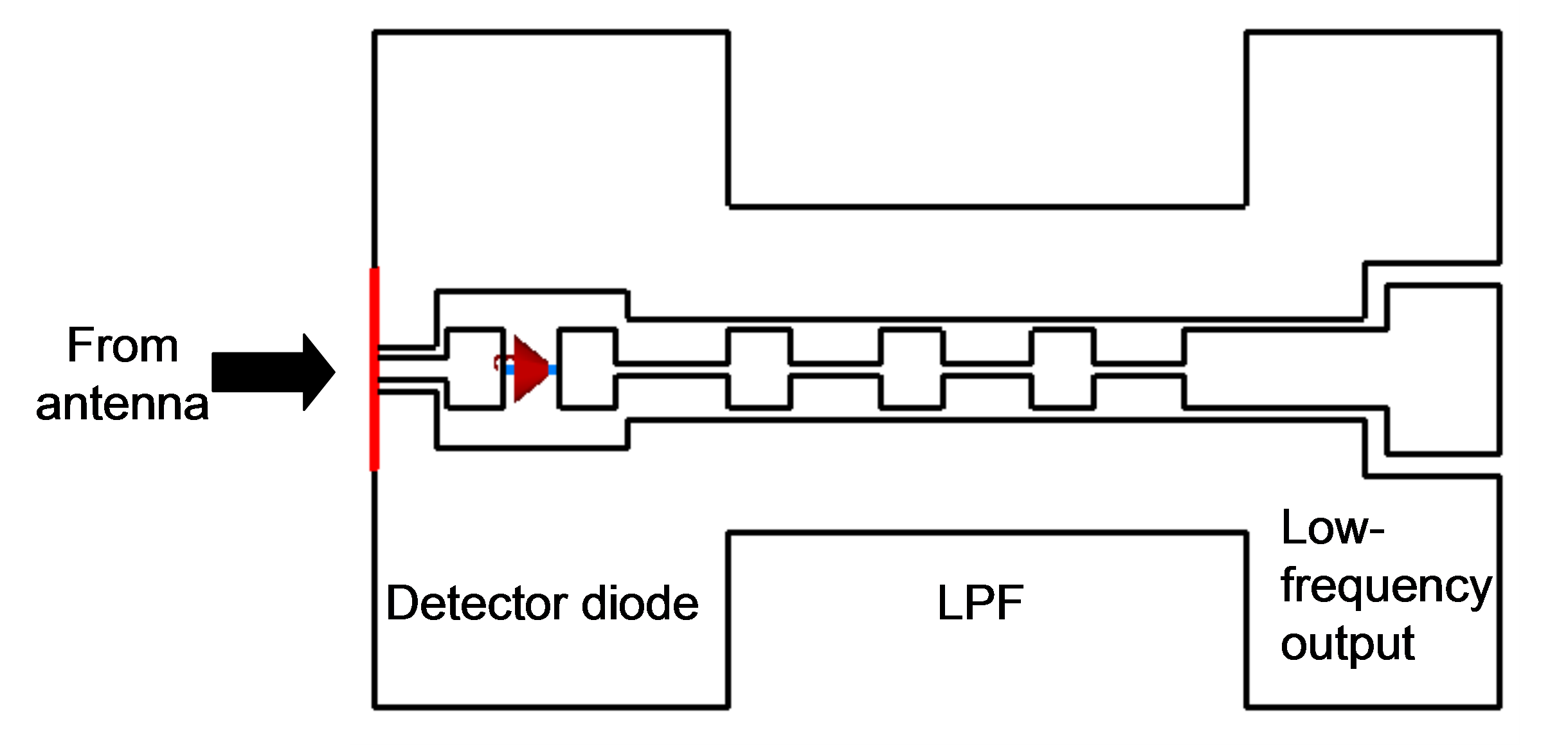
The block scheme of the imaging sensor is shown in Fig. 1. It includes the antenna, the low noise amplifier (LNA), the detection circuit and the low-pass filter (LPF). The antenna receives the signal propagated through free space, acting as an interface between free space propagation and guided propagation through transmission lines. In Fig.1 the signal is amplified by an LNA, but imaging sensor configurations without LNAs are also possible. The millimeter wave signal is then detected. The output is a DC voltage proportional with the power of the detected signal. The low pass filter selects the DC and low frequency components and reflects the millimeter wave signal back to the detecting diode. The output signal (Vout) is then picked up and processed by the external signal processing system.

Fig. 1 Block scheme of the millimeter wave imaging sensor
3. Fabrication and hybrid integration of the component blocks
The antenna structures reported in the previous phases (folded slot antennas and substrate integrated waveguide antennas with operating frequencies of 35 GHz and 94 GHz) were used in the hybrid integration process.
The 3x1 folded slot antenna array was integrated with a diode detector. The detector includes a matching network, composed of a line-stub-line section, and a low-pass filter. The stub of the matching line is symmetric and ends in a short-circuit ensuring a DC return path for the diode. The filter consists of four cascaded high-impedance (high-Z) and low-impedance (low-Z) sections, in CPW technology. The output of the filter is connected to a pad that allows the mounting of a SMA coaxial connector.
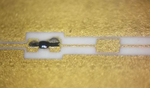
A hybrid integrated diode detector was designed for the SIW fed LTCC antenna, operating at 35 GHz. The length of the CPW transmission line connecting the detector to the transition to the SIW line that feeds the antenna is an important optimization parameter. The detector includes the CPW low-pass filter made of high-Z/low-Z sections. The layout of the detector is shown in Fig. 2 (a). A detail of the hybrid integrated detecting diode is shown in Fig.2 (b). The diode was connected using silver epoxy paste.
(a) |
(b) |
Fig. 2. (a) General layout of the detection circuit; (b) detail of the hybrid integrated diode