Principalele rezultate obtinute in 2016
1. Introduction
During the last phase of the project, Schottky diode test structures were designed starting from the equivalent small signal circuit and finally using partial differential equations. An on-wafer/cable based 2D radiation characteristic measurement system was developed for the millimeter wave antennas. The antennas developed during the previous phases were characterized in terms of the E and H planes. Receivers based in membrane supported antennas and antennas in the LTCC technology were hybrid integrated and characterized.
2. Schottky diode test structures
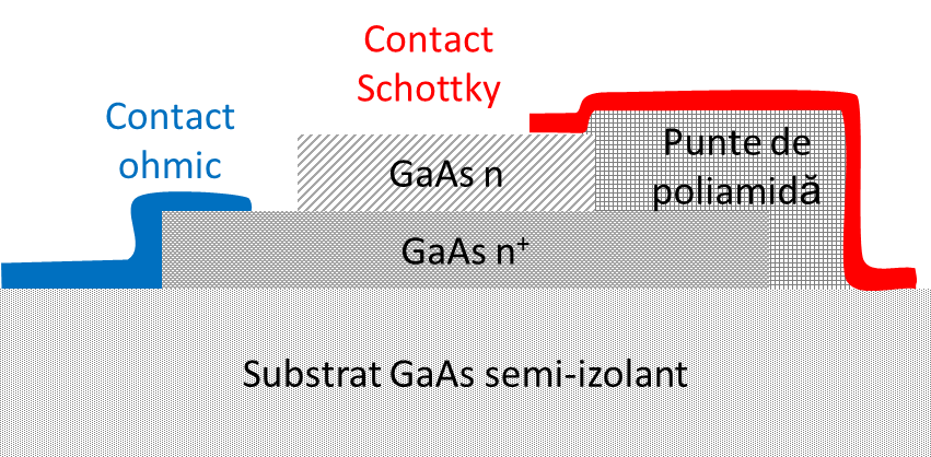
A section through the diode structure that was investigated is shown in Fig. 1 (a). Two GaAs layers with different doping levels - for the ohmic and Schottky contacts - are grown on a semi-insulating GaAs substrate using MBE (Molecular Beam Epitaxy). The two layers are 0.3-0.6 µm thick. These values are selected both due to technological constraints and optimization of the diode performance. The n+ layer where the ohmic contact is placed has an initial thickness of 0.5 µm, with 0.1 µm “lost” during the etching of the mesa structure for the lower doped layer. The doping level of this layer should be as high as possible, in order to reduce the series resistance of the diode, but the MBE technology imposes a maximum limit of 1e18 cm-3 (without ionic implantation). For the lower doped layer, the donor impurity concentration was of 1e17 cm-3, which is sufficient for a good Schottky contact. To connect the Schottky contact in the circuit without shorting to the highly doped layer, a 2 µm thick polyimide bridge was employed.
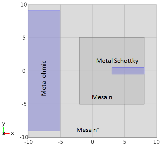
Fig.1(b) shows the top view of the Schottky diode structure described above. The semi-insulating GaAs layer is replaced by isolator-type boundary conditions. Only the contact areas for the metallizations of the two electrodes of the diode are modeled. The areas corresponding to the mesa etching for the epitaxial n and n+ layers are visible.
(a) |
(b) |
Fig. 1 (a) Section through the Schottky diode; (b) top view of the structure
The necessary masks were fabricated and a first run of Schottky diode test structures was processed. Fig. 2 shows an optical photo of a detail of the fabricated structure. The areas obtained through mesa etching, the metallized areas and the area corresponding to the polyimide bridge are visible. The diodes were integrated with pads needed for DC characterization and microwave characterization.
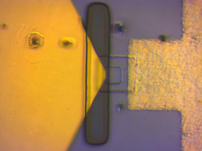
Fig.2. Example of fabricated Schottky diode test structure: optical photo
The fabrication yield of the test structures was relatively low, so only DC measurements were possible at the moment. A measured i/v characteristic in semi-logarithmic scale is shown in Fig. 3.
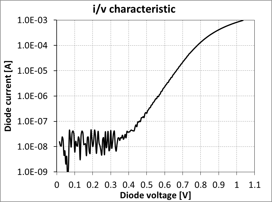
Fig. 3. Measured i/v characteristic in semi-logarithmic scale
3. Radiation characteristic measurements
The photo of the measurement setup is shown in Fig. 4 and consists of a millimeter wave source connected to a standard gain horn antenna, as emitter. A rectangular amplitude modulated (AM) millimeter wave signal is transmitted towards the test antenna (AUT), which is used as receiver. The AM signal is extracted by the diode. The detected signal is then picked up from the support PCB through coaxial connections (SMA or U.Fl) and plotted on a digital oscilloscope. To amplify the received signal, before plotting it on the oscilloscope, a low noise amplifier with controlled bandwidth can be used. This technique can be used to determine the radiation characteristics corresponding to the E and H planes by measuring the received power at different incidence angles.
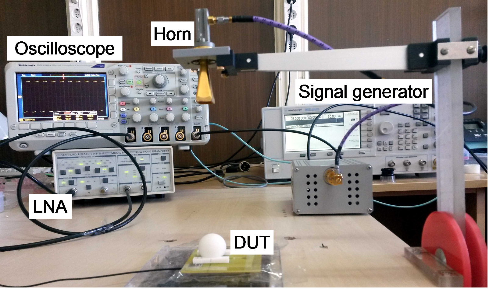
Fig. 4. 2D radiation characteristic measurement system for receiver structures
Caracteristicile de radiaţie ale antenelor LTCC şi pe membrană au fost măsurate şi comparate cu simulările, fiind în bună concordanţă. Ambele tipuri de antene pot ajunge până la câştiguri de 25 dBi în combinaţie cu lentile dielectrice.
4. System characterization: sensitivity measurements
The passive imaging sensors have a direct conversion receiver configuration based on the following principle: the input power propagates through free space and is received by the antenna and transferred to a planar transmission line; the signal is then converted into a DC/low-frequency (video) signal by the non-linear characteristics of the detector diode. A low noise amplifier can be inserted between the antenna and the diode. The signal is picked up from the chip by means of gold wires (wirebonding) and transferred through coaxial cables to the low-frequency electronics, consisting of a low-noise video amplifier and the digital oscilloscope.
The block diagram of the signal generation system is shown in Fig. 5. Besides the equipment described above for the 2D radiation characteristic measurement system (the signal generator with extension module up to 110 GHz and the horn antenna) a tunable W-band attenuator is also needed to control the power level. Thus, the isotropic input power (Piso) can be defined at the reference plane of the antenna.
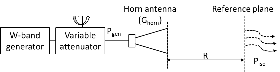
Fig. 5. Block diagram of the signal generation system
The main parameters used to characterize the receiver performance are the isotropic voltage sensitivity, the isotropic tangential signal sensitivity (TSSiso) and the noise equivalent temperature difference (NETD).
NETD values of 1.1 K for the LTCC with SIW receiver and 0.5 K for the receiver with the 2x1 folded slot antenna hybrid integrated with a W-band LNA, a Schottky diode and a dielectric lens, for an integration time of 1 ms were obtained.
It should be noted that these values are comparable to the latest commercial systems, based on massive and high cost horn antennas and rectangular waveguides.