Laser microengraving system
Laser microengraving system:
Performance:
An in-house made laser microprocessing facility, starting from a high-power ps laser at 29 ps pulse duration, 266 nm wavelength, 10 Hz repetititon frequency, 600 MW peak-power per pulse. At the present, the system accepts computer control and may micro-engrave manually or in an automated manner (using AutoCAD software for pattern design) the patterns desired by the beneficiary. Some photos are given below:
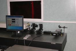
Setup of the system.
The system will be completed with optics for a better control of the beam shape.
Results obtained with the system:
- Up to now we have used the system for engraving Si, Ge, thermally-grown SiO2, Cr/SiO2, glass, SiC.
- In some cases, structures at the nanoscale have been obtained, as shown in the image below:
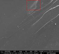 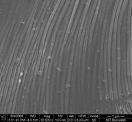
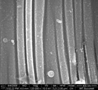
SEM image of the Si surface irradiated with high-power UV pulses. The red rectangle is the region augmented in the central and left figures, respectively. The Si wires have less than 130 nm diameter, are curved and form bundles.Their lengths are between 10 microns and several tens of microns.The bar scale in the right image is of 400 nm. SEM image by courtesy of Adrian Dinescu, IMT-Bucharest.
|