Original concepts developed in the field of additive manufacturing and nanolithography:
1. 3D Printing at micro-nano scale (international patenting) – it is technology that uses the optical control of the liquid exiting the tip of a fountain pen cantilever on the substrate’s surface. The control is achieved by carefully adjusting the viscosity of the exiting liquid. The light can either gradually photopolymerize or gradually photoevaporate the solvent in the liquid solution. A higher illumination promotes faster reticulation / evaporation, thus increasing viscosity very fast and denying the liquid to spread too much on the surface. A lower illumination intensity produces a less accelerated process of viscosity increase and thus the liquid is allowed to diffuse more over the surface. By moving the cantilever along the X, Y, Z directions, 3D structures with few tens of nanometers can be built.
2. 3D Printing with focused beams of ultrasound (international patenting) - The technology makes use of a focused ultrasound beams for locally and selectively welding a bed of compressed powder. By scanning the focus along the XYZ directions, the 3D object is created. Once finished, the object is removed from the powder bed and depowdered. It is a room-temperature process that does not need support structures like in the case of commercially existing 3D Printing techniques such Selective Laser Sintering / Melting (SLS/M) or Direct Metal Deposition (DMD/LENS). This is due to the fact that it is an ambient temperature process and, respectively, that the powder bed is compressed by a piston, compression that makes practically impossible any deformation of the part that is constructed.
The process is applicable to a wide palette of materials – all materials that are weldable by ultrasound are usable for this process. Not only the technology allows the use of single materials, but also combinations of powders from different materials can be used, as shown in figure below.
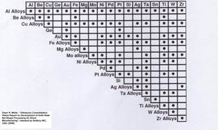
Graphs showing compatibility of materials for ultrasound welding. Left – the case of metals; Right – the case of polymers. The squares marked with colour show compatibility between materials corresponding to the intersecting column and, respectively, row.
Except of the materials shown above, glass and some ceramics can also be welded by ultrasounds, as well as metal-ceramic composites and polymer containing different types of fillers (carbon fibre, graphene, etc.). There are also reports that basalt can be ultrasonically welded. This is a very important material since the lunar regolith has a composition quite similar to basalt.
The working principle of ultrasound welding is as follows: the ultrasounds put the grains into relative movement one to each other. This has as effect the surface smoothening, grain deformation and, in some cases, the local melting of the material (more in polymers than in metals). Except of these processes, atomic inter-diffusion between adjacent grains takes place, creating the weld. This is a very general and brief description of mechanisms taking place at the interface between powder grains. For each type of material some of these mechanisms dominate and other new mechanisms can also appear. The powder is compressed because of two reasons: a) to ensure a good acoustic coupling between powder grains; b) to densify the material as close to the full density as possible. However, the compression is not so large so as cold sintering appears.
3. Simultaneous and independent controls of cantilevers in array comprising up to few millions of cantilevers (private communication) – It is a concept allows the independent and simultaneous control of each cantilever in an array comprising up to few millions cantilevers from the desk of a common PC. Useful in nanolithography and nanotechnology at industrial scale.
4. Multi-role chip for advanced 2D and 3D nanolithography (patenting) – It is a chip that allows implementation of several nanolithography techniques, including nanoscale characterization, in such a way so as to avoid cross-contamination from one sample to the other. All the ensemble is controlled from a single PC.