Results
2016 - Objective: optimized UV photodetector structures characterization----------------------------------
MSM photodetectors on GaN membranes optimization; photodetector structures characterization
The MSM photodetectors on GaN membranes optimization optimization has been performed on comercial GaN/Si wafers (purchased from NTT AT Japan). For the MSM structures optimization process Electron Beam Lithography with “direct writing “ has been used.
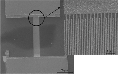
Fig. 1 SEM photo of a photodetector structure supported on thin GaN membrane, with digits/interdigits width of 100 nm
Dark current measurements
The measurements of dark current dependence with the applied voltage for photodetector on membrane structures have been performed with a Keythley 4200 equipment. At 2 volts polarization, the dark current value is 4.35 pA, for optimized structures with 100nm digits (Fig. 2)
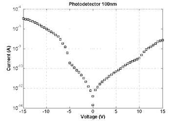
Fig.2 Dark current dependence of applied voltage for structures with 100 nm digit/interdigit
For all photodetector structures, the dark current grow with the digit/interdigit space reduction has been observed. Also, a significant grow of the dark current as well as the d(logI)/dV slope for 0.5 µm at applied voltage over 5 V.
In the case of photodetectors on GaN membranes, the photogenerated carriers are blocked in the very thin membrane , therefore the carrier flux is inhibited at a moderate applied voltage and the dark current as well as the responsivity improve.
Responsivity measurements
Measurements for responsivity have been performed using a special equipment for the frontside as well as the backside illumination (Fig. 3).
The MSM structure total area was 10000 µm2 (digits plus interdigits distances for both structures) and the active area without metalisation was 5000 µm2.
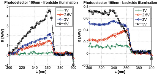
Fig. 3 Responsivity dependence of wavelength at frontside illumination (a) and backside illumination (b) for optimised UV photodetector, digit/interdigit width of 100 nm, at different polarisation: 1 V, 2.5 V, 3 V, 5 V
The maximum responsivity was obtained for wavelength l = 362 nm.
For structures having digit/interdigit space of 100 nm , responsivity at frontside illumination was 1.45 A/W, at the backside illumination was 0.37 A/W. For structures having digit/interdigit space of 200 nm, maximum responsivity at frontside illumination was 0.127 A/W, at the backside illumination was 0.022 A/W. These data correspond to a ratio frontside illumination versus back side illumination of 3.9 for the first structure and 5.9 for the second structure, respectively.
Resonance frequency dependence with pressure for SAW on GaN structures
Fig. 4 SAW structure with 200 digiţi/interdigiţi (a); metalic support for SAW structure (b)
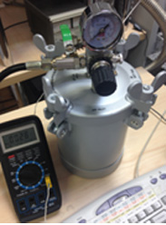
The dependence of resonance frequency with applied pressure has been measured using a controlled pressure chamber (Fig.5, 6).
 |
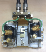 |
| Fig. 5 controlled pressure chamber | Fig. 6 In-house on-wafer S parameter measuring set-up |
The resonance frequency dependence of pressure, in the range 1 – 5 Bar, is extracted from S11 parameter (fig.7). In figure 7a, the decay of the SAW resonance frequency with the pressure is illustrated.
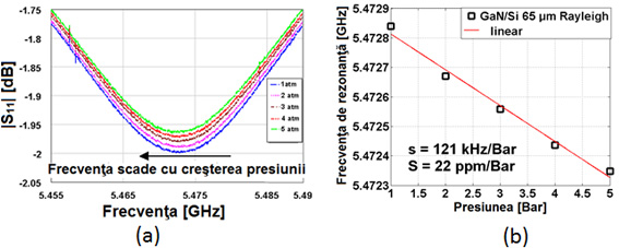
Fig. 7 The resonance frequency dependence of pressure (a); liniar dependence aproximation (b)
Due to the promissing results, a new SAW structure on membrane, with Si substrate of 10-20 μm has been designed and fabricated. The GaN/Si wafer has been thined from 525 μm to 100 μm, and sbsequently selective etched by RIE. We have obtained a GaN/Si wafer having 10 - 20 μm thickness only under the active area of the SAW’s (area with the IDT structure) .
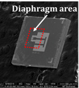
The SAW structure suspended on 11.2 μm thick membrane is presented in fig. 8.
The reflection S11 parameter variation with resonance frequency presents two resonance peaks, therefore two propagation modes: Rayleigh mode (the phase velocity, v=λf is about 4000 m/s) at 5.24 GHz and the Lamb mode at 9.61 GHz, typical to membrane supported SAW structures (Fig. 9)
 |
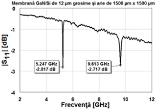 |
Fig.8 SEM image for SAW |
Fig. 9 Resonance frequencies for one port SAW supported on GaN/Si (1.2 μm /10 μm) membrane |
The resonance frequency shift vs. pressure was analyzed for both peaks and for both structures using a in house on-wafer setup introduced in a in-house pressure chamber (Fig. 5 and 6) for 1-5 bar range. The measurements for the Rayleigh propagation mode are presented in figure 10. The obtained sensitivity was 92 ppm/bar.
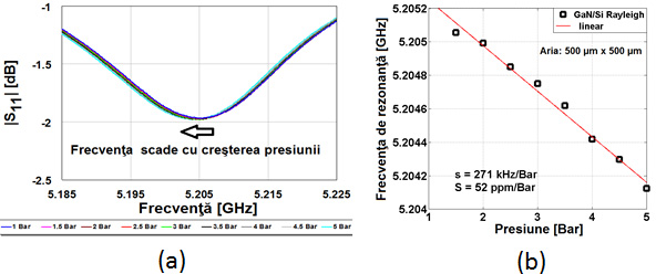
Fig. 10 Frequency shift vs. pressure (left) and pressure sensitivity results (right) for Rayleigh mode of SAW resonator wth 500 µm x 500 µm aria
For the Lamb propagation mode, in the pressure range of 1-5 Bar, the frequency variation is presented in fig 11a, resulting a sensitivity of 159 ppm/Bar, 1.7 times higher then the sensitivity in the Rayleigh propagation mode (fig.11).
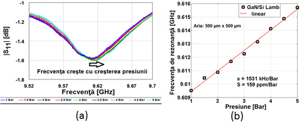
Fig.11 Frequency shift vs. pressure (left) and pressure sensitivity results (right) for Lamb mode of SAW resonator wth 500 µm x 500 µm aria
The novel SAW pressure sensing structures have demonstrated high values for the sensitivity, higher then the values reported in the literature for AlN layer on 50 μm Si substrate – for the Rayleigh mode -3.33 ppm/Bar and -9.07 ppm/Bar for Lamb mode. For our structures, the measurements have demonstrated that the Lamb mode is more sensitive with the pressure then the Rayleigh mode.
2015 - Objective: Technological precessing and the characterization of new UV detecroe based on SAW resonator.
This stage of the project aims at the interaction of a photodetector and a SAW structure obtained on a common substrate, in the proximity of the photodetector. This interaction can be observed in the both directions: lightening the photodetector influence SAW properties (a); SAW polarization influence the photodetector (b) (fig. 1). At this stage, we have annalised the interaction (a). The SAW structures operating at frequencies over 6 GHz have been manufactured on GaN/Saphire (GaN thickness of 0.3 μm) using nanolithography in order to obtain IDTs and reflectors with 200nm width, dimenssios requested for the SAW resonance frequencie > 6GHz.
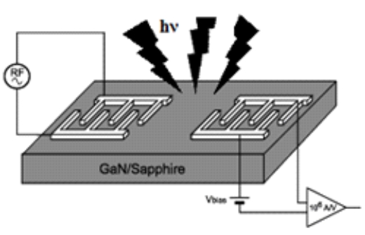
Fig.1. Scheme of the SAW-photodetector interaction (a and b)
Masks for SAW structures having interdigits of 200 nm and 300nm, on GaN (0.3 mm) on Saphire (525 mm). IDT’s length is 50mm. Structures are type « face to face ».
Mask 1 is designed to obtain the pads contacts, then folows the direct rithing by advanced nanolithography with electron beam (EDL). In order to delimitates the IDTs, a lift-off process was used with Ni/Au (5/10 nm) metallization.
Mask 2 (overlay) is designed to thicken the contact pads in order tu secure the contact between the pads and the nanolitographic lines-200nm Au.
The tehnological manufactured structures have been morphologicaly characterised with the scaning electron microscope TESCAN (fig. 2)
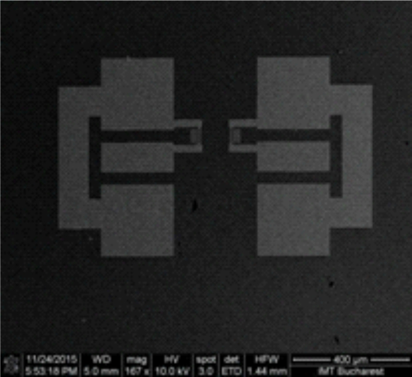
Fig.2. SEM image of the SAW-photodetector structure having two IDTs « face to face » at a distance of 100 mm
The characterization of SAW/photodetector structures – UV interaction. Experimental results
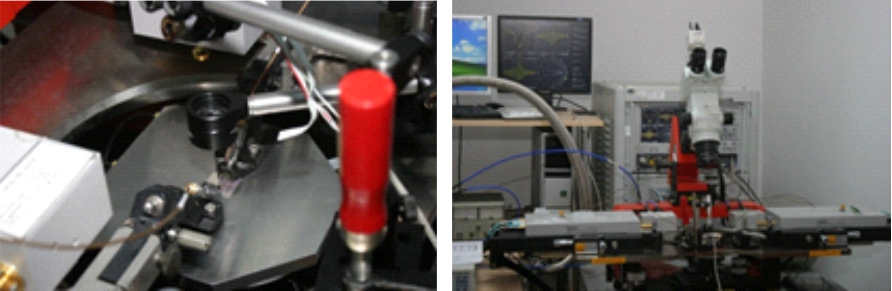
Fig.3. Experimental set-up for characterization of SAW/photodetector structures – UV interaction
Left: optic set-up for UV illumination
Right: microwave equipment to generate the signal in SAW resonator and S11 measurements
SAWs resonators response at UV illumination with wave length of 341 nm) represent a resonance frequency shift, from 6.63 GHz to different values (figure 4), depending also of the UV power density –ilustrated in figure 5.
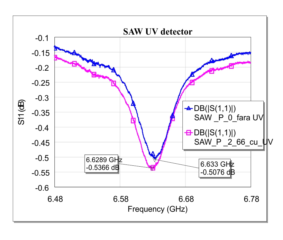
Fig.4. Comparative S11 measurements for detector with SAW resonator nonilluminated and illuminated with UV ligth having 2.66 µW/mm2
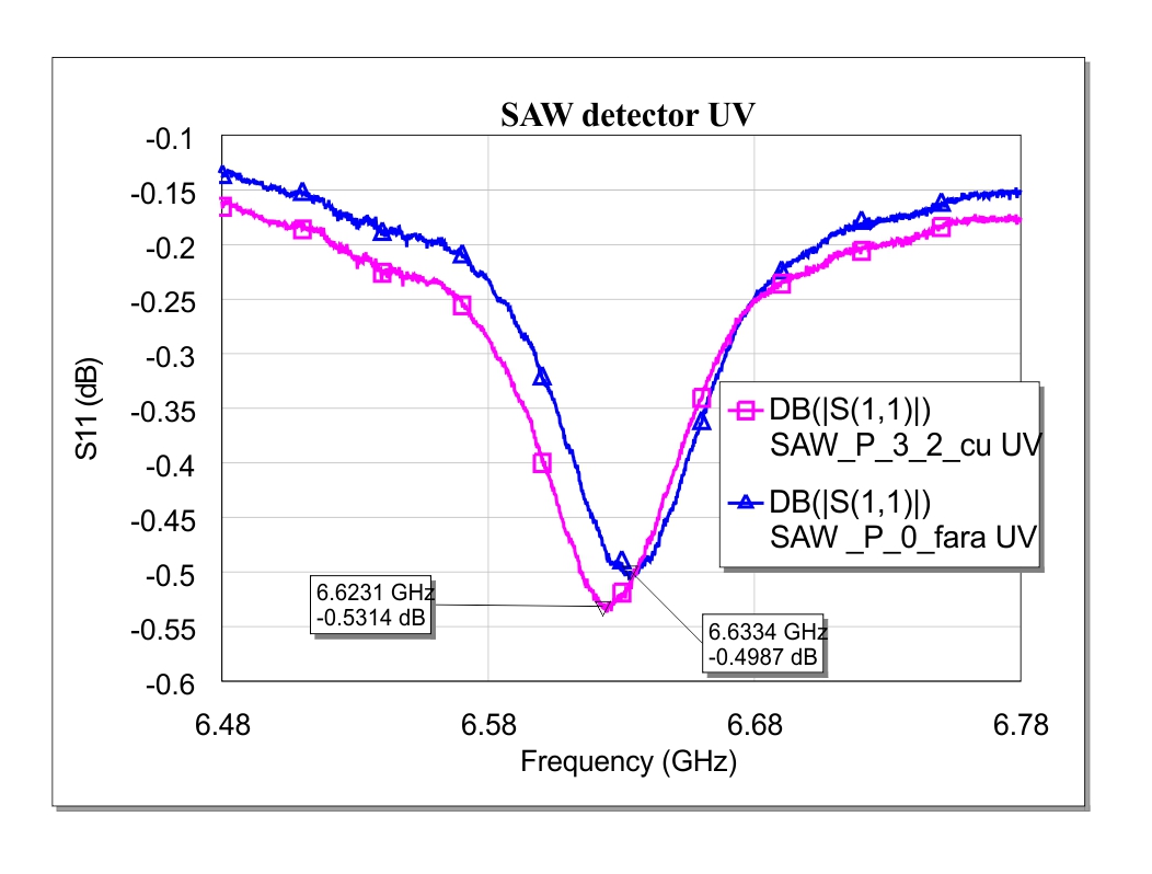
Fig.5. Comparative S11 measurements for detector with SAW resonator nonilluminated and illuminated with UV ligth having 3.2 µW/mm2
2014 -------------------------------------------------------------------------------------------------------
The optimization of the MSM interdigitated photodetectors structures
In order to optimize the MSM (metal –semiconductor-metal) interdigitated photodetectors structures a new run was processed on commercial GaN/Si wafers (from NTT AT Japan) having the GaN layer grown by MOCVD. The un-doped GaN layer 0.5µm thick was grown on high resistivity <111> silicon. The buffer layer between GaN and silicon has 0.28 µm. The total area of the MSM structure is 2000 µm2 but estimating a 50% transparency of the contact, the active area was about 1500 μm2 .. A SEM image of the MSM structure is presented in fig 16 and details in fig 17.
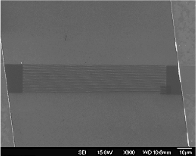
Fig 16. SEM image of the MSM structure processed on thin GaN membrane having 0.5 µm wide digit/interdigit
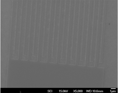
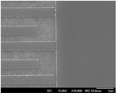
Fig 17 Details of the MSM photodetector structure processed on GaN membrane
The dark current and the responsivity were measured before and after membrane formation for voltages up to 10 V. The dark current for the bulk device was around 1 pA at 2V while in the case of the membrane device was about 10 pA. The dark current vs applied voltage is prezented in Fig 18.
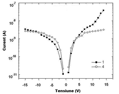
Fig 18 The dark current vs applied voltage for two structures manufactured on GaN membrane
The responsivity as a function of the photon wavelength was measured using an Ozone free 150W Xe-lamp UV light source from Hamamatsu. We have used low noise amplifiers to measure all the spectra. The results are presented in Fig. 19 and 20.
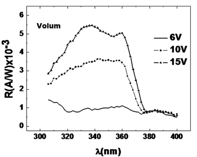
Fig. 19 Responsivity vs wavelength for the UV detector structure before the silicon substrate removal
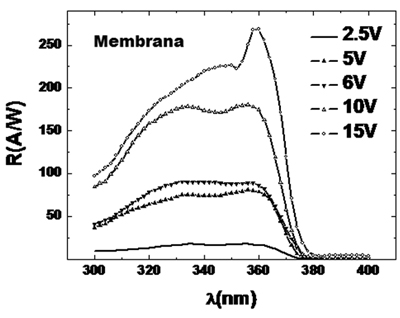
Fig. 20 Responsivity vs wavelength for the UV detector structures manufactured on thin GaN membrane
Nanolithographic processes for MSM structures and IDT’s manufacturing on GaN for SAW resonators and photodetectors
Nanolithographic lines on GaN/Si test structures were processed. Continuous metallic Ti/Au path were obtained for interdigitated structures having 70 – 200 nm width.
The very thin digit interdigit spacing width obtained for the IDTs manufactured on GaN represents the actual state of the art. The nano-lithographic process on GaN represents a major challenge due to the charging effects as well as due to the major difficulties to lift off the gold metallization because of the high atomic mass of the Gallium.
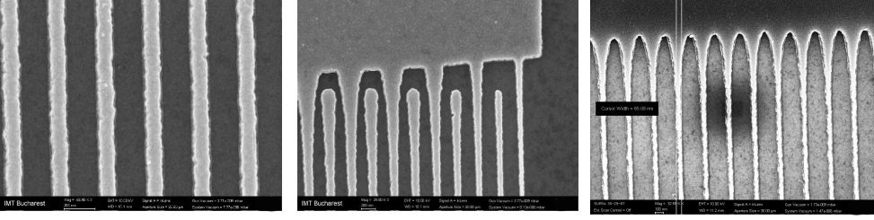
Fig 1 Fig 2 Fig 3
Fig 1 Nanolithography on GaN (digit/ interdigit spacing 150nm and 100 nm metallization thichness
Fig 2 Nanolithography on GaN (digit/ interdigit spacing 100 nm and 50 nm metallization thichness)
Fig 3 Nanolithography on GaN (digit/ interdigit spacing 70nm and 30 nm metallization thichness
Manufacturing of SAW “face to face” structures on GaN/Si working in the X-band (8-12 GHz)
The first processed SAW structures were “face to face” resonators. The first step for the X band resonator manufacturing represents the photolithographyc process for contact pads definition A Ti/Au sandwitch (10nm/200nm) has been used for the pads. The interdigitated transducer was manufacurd using Electron Beam Lithography (EBL). The obtained structures and the electrical measurements are presented below. The structure had 100 digits/interdigits with 100 µm length.
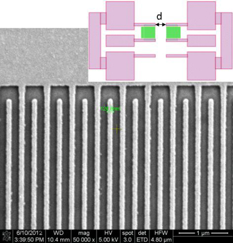
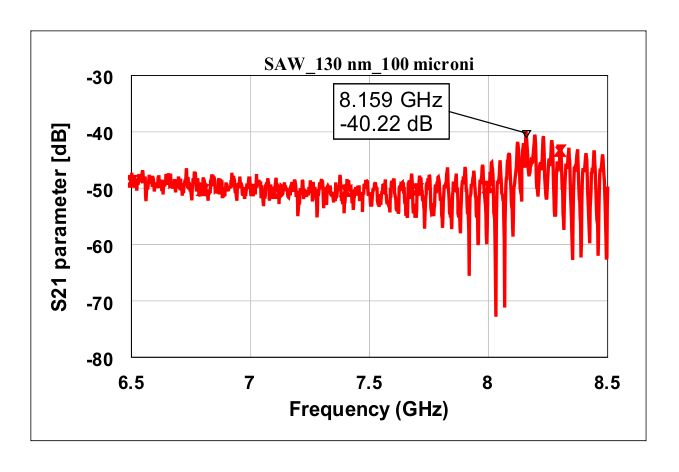
Fig 4 Details of the “face to face” SAW resonators having 130 nm digit/interdigit spacing. The distance between IDTs is d = 100 µm. The inset presents the layout of the structure
Fig 5 Measured S21 parameter for the “face to face” SAW resonators. The distance between IDTs is d = 100 µm.
GaN membranes
Two types of GaN metalized membranes have been processed by micromachining of GaN/Si. Dimensions and metallization topologies were different. At the A type structures the membrane area was smaller and the metalized areas were interdigitated type. “Pad” type metalized structures were manufactured partial on the future membrane. The area of the B type membrane was bigger and the metallization was compact on two regions of the future membrane. Manufacturing and characterizations of those membranes represent the first step for future suspended UV photodetectors.
After top metallization, the membranes were processed using double alignment techniques and selective RIE etching. The GaN membranes had 0.4-0.5 μm thickness.
Morfological characterization of very thin GaN membranes
Membrane deflection analysis was performed with 3D WLI Photomap equipment. The deflexion versus position (A1-A1 direction and A2-A2 direction) is presented in fig 6 and 7 for A respective B type structures. The main conclusion was that the A type structure has smaller deflection and is proper to be used in suspended UV photodetector manufacuring. Also an important result was that the menaining of the pads outside of the membrane can reduce the deflection.
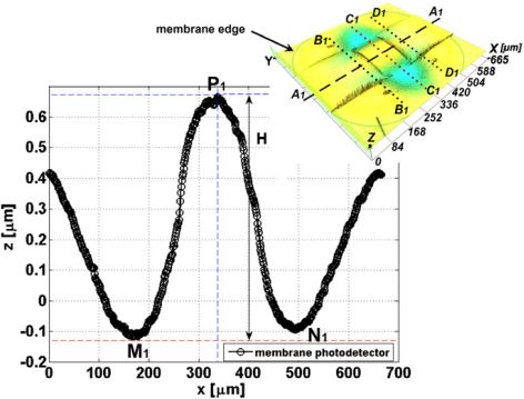
Fig 6 Membrane ( type A) deflection on x direction; the inset represents the structure 3D topography (10/200 nm Ni/Au metallization)
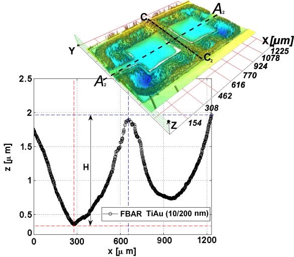
Fig 7 Membrane ( type B) deflection on x direction; inset with structure 3D topography (10/200 nm Ti/Au metallization)
Manufacturing and characterization of single resonator SAW structures
The SAW structures (single resonator type) were manufactured on GaN/Si wafers purchased from NTT AT Japan (the thickness of the GaN layer was 1 µm and the total thickness of the buffer layer was 0.2 µm). The single SAW resonator has the advantage of high Q.
The “face to face” resonators are characterized using the transmission parameter S21 and shows much higher losses than for the “single resonator” structures characterized through the reflection parameter S11
For the IDT structure, direct writing Electron Beam Lithography (EBL) was used:
- Digit/interdigit width130nm; digit length 100 µm, 50 µm
- Ti/Au metallization 100 nm
- IDT with 150 digits/interdigits
- Reflectors with 50 digits/interdigits
In order to obtain resonance frequency around 8.5 GHz in the next step, it is necessary process IDTs with digits/interdigits having 120 nm witdh.

Fig 8 SAW resonator layout ("single resonator")
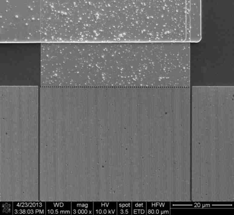
FIg 9 SEM image of the single resonator SAW structure (detail of the IDT)
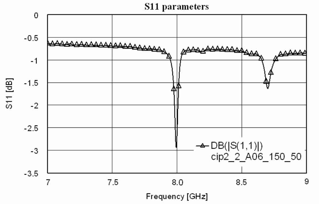
Fig 10 S11 parameter for SAW resonator
Manufacturing and characterization of the UV photodetector
The MSM (metal –semiconductor-metal) interdigitated photodetectors structures were manufactured on GaN/Si thin membranes (wafers purchased from NTT AT Japan ) having the thickness of the GaN layer 0.3 µm and the total thickness of the buffer layer AlN and AlGaN 0.2 µm. The diport type pads were deposited by a lift-off process of Ni/Au (20nm /500 nm). The interdigitated MSM structure was processed by direct writing on the wafer using Electron Beam Lithography (EBL “e_Line”, e-beam lithography equipment from RAITH GmbH). 200 nm digits/interdigits width and 100 µm were processed.
The semitransparent Ni/Au metallization Au (5nm /10 nm) was processed by lift-off. The silicon substrate was then thinned down to 150 µm. For the formation of the membranes, an Al mask was patterned and deposited on the back side, to serve as an etch mask for the reactive ion etching (RIE) process (300 µm x 300 µm).
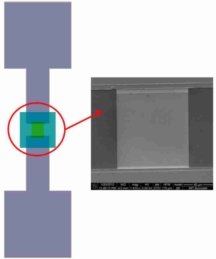
Fig 11 Photodetector layout having 200 nm digits/interdigits witdh (the detail present o SEM image of the IDT)
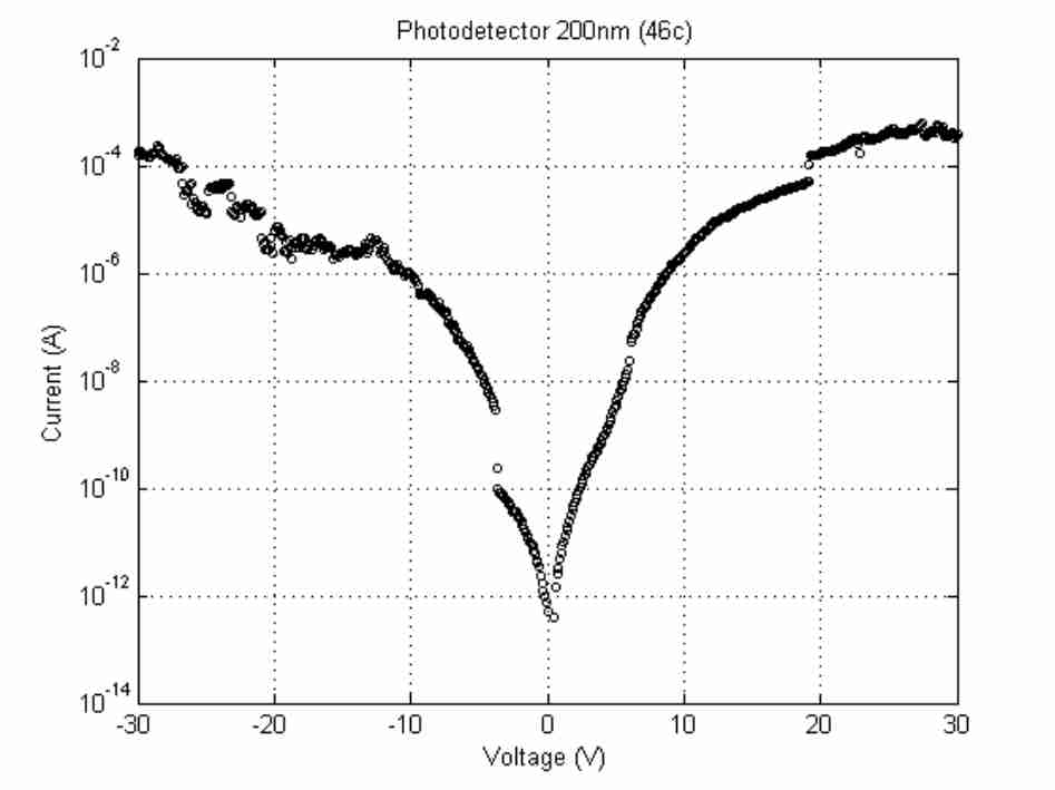
Fig 12 Dark current vs applied voltage for the UV photodetectors; digit/interdigit 200 nm witdh
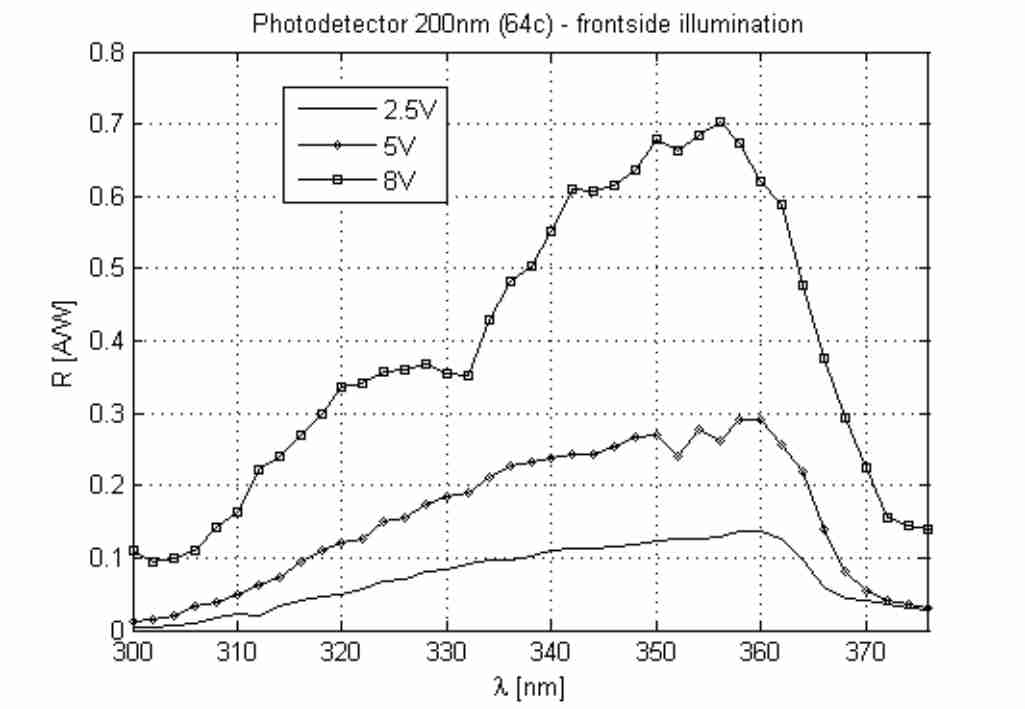
Fig 13 Responsivity vs. wavelength for front side at front side-illuminated UV photodetector structures with digits and interdigits 200 nm witdh, at bias of 2.5 V, 5 V, 8V.
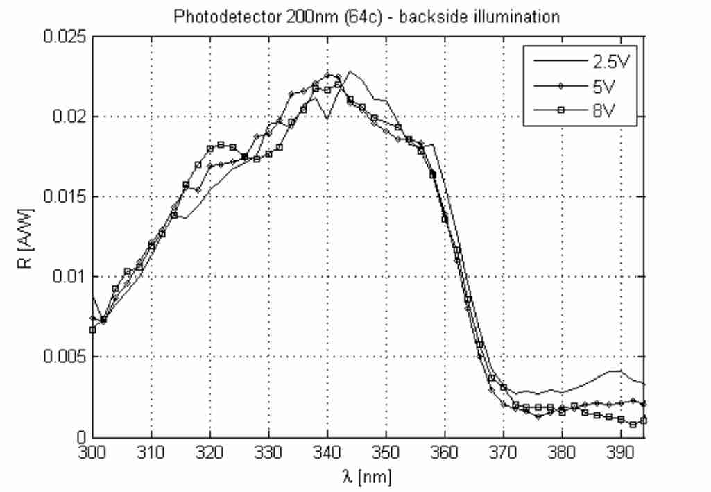
Fig 14 Responsivity vs. wavelength for front side at back side-illuminated UV photodetector structures with digits/interdigits / 200 nm witdh, at bias of 2.5 V, 5 V, 8V.
Micro-Raman spectroscopy used to characterize the in-plane stress in the suspended on GaN membrane photodetector structures.
There is a linear relationship between the residual stress σxx and E2 (high) Raman shift Δω=Kσxx. with K value of 4.3 cm−1/GPa.
Raman spectra were acquired in backscattering geometry using a LabHR 800 spectrometer, at a 632 nm laser excitation. The free-stress frequency of 568 cm−1 for bulk GaN crystal was used as reference value (zero stress).
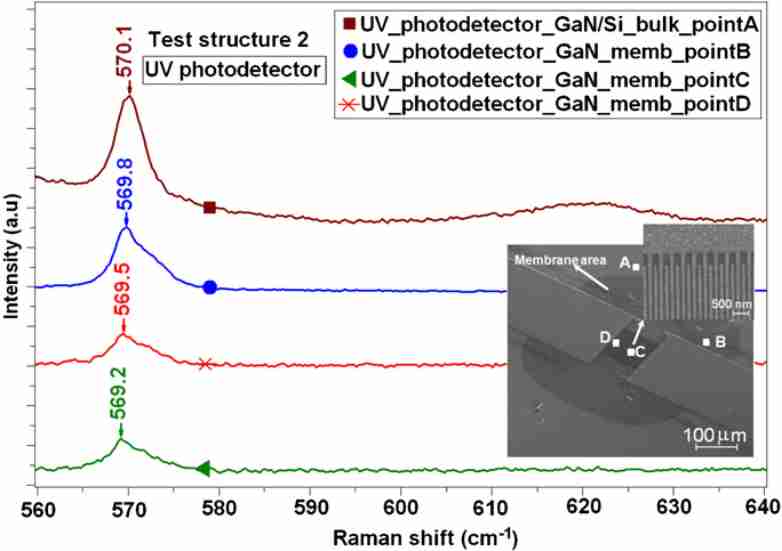
Fig 15 Raman shift for different regions of the UV photodetector structures manufactured on the 0.5 μm thin membrane )[A Cismaru, A Muller, G Konstantinidis, F Comanescu, M Purica, A Stefanescu, A Stavrinidis, A Dinescu, A Moldoveanu, “Residual stress distribution and deflection analysis of very thin GaN membrane supported devices”.J. Micromech. Microeng. 23 (2013) 015010]
On the unreleased region of the UV photodetector structure (point A, inset of figure) resulted to stress frequency at 569.8 cm−1 corresponding to a compressive stress of 418 MPa. Measurements performed on the edge of the membrane (point B, inset of figure) exhibited 569.5 cm−1, (348 MPa) while in the centre of the membrane, in the region of the nanometric MSM structure (point D, inset of figure) displayed stress frequency at 569.3 cm−1 (300 MPa)