| Information Technology and Communications, Space and Security |
GaN based single resonator SAW structure operating in the GHz range, for temperature sensing |
Competency:
Smart specialization: |
Micro-and nano-electronic devices
Information and Communication Technologies |
| |
TRL 3 research to prove feasibility / Experimental and characteristics proof of concept
Contact Person: Dr A Muller, [email protected] |
| |
The resonators were manufactured by L4 in IMT in the frame of the European FPT IP Project No 288801 - «Smart integration of high power electronics for industrial and RF applications SMARTPOWER» 2011- 2016. The project is coordinated by Thales TRT, France, and IMT is partner together with other 14 partners.
The GaN SAW temperature sensor is solution for temperature monitoring of GaN based transceiver circuits and also for other applications. The structure is compatible with wireless data transmission and with monolithic integration with the GaN based transceiver circuit.
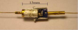
GaN based single SAW resonator temperature sensing structures, having IDTs with fingers /interdigit spacing of 200 nm, 170 nm, 150 nm and 120 nm widths have been manufactured. The IDTs have 150 digit and interdigit spacing, 100 µm long. Reflectors having 50 fingers and 50 interdigit spacing have been placed, on each side of the IDTs at 0.95 µm distance from the IDT.
 |
(a) SAW single resonator structure with 150 digits/interdigit spacing and 170 nm figer/interdigit spacing width; the inset presents the entire structure including the connection/measuring pads;
(b) Detail of the nanolihographic process for the structure with 120 nm finger/interdigit spacing width. [A. Muller, International Microwave Symposium -IMS 2014, 1-6 June, Tampa, USA pp 46-48] |
|
W-Band hybrid integrated direct detection receiver for space applications
|
Competency:
Smart specialization: |
Micro-and nano-electronic devices
Space |
| |
TRL 3 research to prove feasibility / Experimental and characteristics proof of concept
Contact Person: Dr Dan Neculoiu [email protected], Drd. Alina Bunea [email protected] |
| |
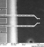
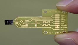
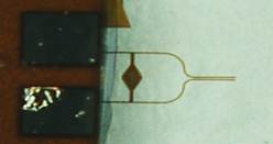
A W-band (75 – 110 GHz) direct detection receiver consisting of a membrane supported folded slot antenna and a detection circuit based on a zero-bias diode (ZBD) was designed and fabricated.
The receiver was designed and manufactured by L4 under the contract STAR No 86 /2013 financed byRomanian Space Agency „ Millimetre and sub-millimetre wave GaAs Schottky diodes, detectors and mixers” Coord. Dr A. Muller, IMT Bucharest (2013-2016)
The antenna is processed on a 2.1 μm thick SiO2/Si3N4 (1.5/0.6 μm) membrane released through deep reactive ion etching (DRIE) of high-resistivity silicon and the detection circuit is processed on silicon bulk.
In order to get a good estimate of the behavior of the receiver at low temperatures, the detection circuit was placed in a cryostat with an on-wafer measurement setup. The i/v characteristic and the detected signal were determined between 295K and 23K.
 |
 |
| Photo of the hybrid integrated direct detection receiver |
Photo of the device under test in the cyostat |
|
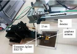
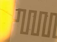
Coplanar patch antenna on graphene
|
Competency:
Smart specialization: |
Micro-and nano-electronic devices
Information and Communication Technologies |
| |
TRL 3 research to prove feasibility / Experimental and characteristics proof of concept
Contact person: Dr M Dragoman, [email protected] |
| |
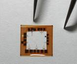
A graphene coplanar patch antenna (CPA) for 10 GHz was processed on high resistivity substrate, as doped Si does not allow operating in microwave antenna due to large losses. Antenna was measured and the radiation characteristic was determined. The antenna is intended to be embedded into a RF transceiver operating at 10 GHz, providing return loss and radiation tunability by the simple application of a DC bias voltage to the graphene footprint. The work was performed by L4 team from IMT.
| The graphene coplanar patch antenna was designed, fabricated and tested in the frame of the European FP7 STREP contract No 318352 – “Carbon based smart systems for wireless applications NANO RF”, 2012-2016.The project is coordinated by Thales TRT, France, and IMT is partner together with other 12 partners. |
 |
 |
| Photo of the wafer with antenna on graphene |
Measuring system |
|
Superconductor YBCO Bolometer
|
Competency:
Smart specialization: |
Micro-and nano-photonic devices
Space |
| |
TRL 3 research to prove feasibility / Experimental and characteristics proof of concept
Contact person: Dr. Mihai Kusko, [email protected] |
| |
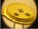
IMT-Bucharest has developed a thermal radiation detector operating at cryogenic temperatures within a STAR project (2012-2014)
The bolometer is based on thin layers of Yttrium-Barium-Copper-Oxide YBCO operating by monitoring the resistance increase with temperature due to the radiation heating. The detector operates at transition temperature where the material goes from the superconducting state to the normal state. The bolometer proposed here may find application in space programs as the Earth observation which includes atmosphere monitoring for the pollutants species as CO, CO2, SO2, CH4, NH3 etc. by recording the absorption spectrum in the wavelength range 3-15 microns since it is well known that many of these species have a strong absorption in this spectral region. IMT (the consortium Coordinator) fabricated the bolometer, whereas National Institute for Laser, Plasma and Radiation Physics INFLPR deposited the YBCO thin layer with the Pulsed Laser Deposition (PLD) equipment and SC Optoelectronica 2001 SA team designed and fabricated the read-out electronic circuits.
 |
Optical image of bolometer based on the YBCO pattern layer
|
|
SOI-based MEMS microgrippers, electrostatically actuated, for pick-and-place operations
|
Competency:
Smart specialization: |
Micro-and nano-electronic devices
Information and Communication Technologies, Space, Security |
| |
TRL 3 research to prove feasibility / Experimental and characteristics proof of concept
Applications: micromanipulation, pick and place, microassembly, microrobotics industry
Contact person: Cătălin Tibeică, [email protected] |
| |
The microgrippers were designed and manufactured by L5 in the frame of the National Romanian program Convert – “MEMS microsystems for micromanipulation in microrobotics”.
These devices were designed in two configurations – tweezers normally closed, and tweezers normally open, with a maximum deflection, measured at the tips, of 25 µm, and an extension of the arms outside of the chip of 300 µm. The actuation mechanism for each arm relies on a lateral comb drive system, and a mechanical compliant amplifier.
The manufacturing processes include front and backside DRIE of an SOI wafer, followed by release of the chips by HF etching of the burried oxide.
The gripper is glued and wire-bonded on a PCB designed to be integrated on a micromanipulation stage.
 |
 |
| SEM image of the microgripper’s arms |
Optical image of the chip mounted on the PCB |
|
| Gas sensor on SiC based on a MOS capacitor |
Competency:
Smart specialization: |
Micro-and nano-electronic devices
Information and Communication Technologies, Space, Security |
| |
TRL 3 research to prove feasibility / Analytical and experimental critical function proof of concept
Contact Persons: Florea Craciunoiu ([email protected]); Razvan Pascu ([email protected]) |
| |
A gas sensor on SiC based on a MOS capacitor was designed and fabricated by L1 in the frame of SiC-GAS PNII-PCCA (ctr 204/2012) project coordinated by ICPE-CA Bucharest.
| SiC MOS capacitors have been tested as hydrogen sensors at temperatures ranging from 25 to 200°C, for different H2 concentrations between 20 to 1800 ppm. It is noticeable that increasing the testing temperatures does not affect the sensor response, being quite the reverse: at 200°C the sensor response reaches a maximum value of 90 % for the lowest analysed concentration (20 ppm of H2). |
 |
|
Polymer-based MEMS microgrippers with embedded microheaters, electrotermally actuated, for bio-micromanipulation and microassembly
|
Competency:
Smart specialization: |
Micro-and nano-electronic devices
Information and Communication Technologies, Space, Security |
| |
TRL 3 research to prove feasibility / Experimental and characteristics proof of concept
Applications: bio-micromanipulation, pick and place, microassembly, microrobotics industry
Contact person: Dr. Rodica-Cristina Voicu, [email protected] |
| |
The polymer microgrippers were designed, manufactured and experimentally tested by L5 in IMT Bucharest in the frame of the National Romanian program Convert – “MEMS microsystems for micromanipulation in microrobotics”.
The microgrippers were designed using the principle of electrically driven thermal actuation in both operating modes: namely normally open operation and normally closed operation. In each design, the microheaters are embedded in two polymer layers for electrically isolation and to improve thermal efficiency.
The microgrippers were fabricated using biocompatible materials, such as SU-8 polymer used as structural layer and based one a wet release using the Omnicoat stripper.
The grippers can operate in different media, such as air or liquids. The tips can have an opening up to 100 µm in air in order to grip and manipulate an micro-object, such as cells, tissues, vessels or MEMS/MOEMS components.
 |
 |
| a)Optical image of an SU-8 microgripper arranged for tests; |
b)Image of a chip with free standing SU-8 and Gold microgripper structures |
| R. Voicu et al, Material Characterizations for MEMS Vibration Sensors and Biostructures Applications, Digest Journal of Nanomaterials and Biostructures 10 3, p. 1077 – 1085, 2015 si M. H. Al-Zandi, R-C. Voicu, R. Muller, C. Wang, Testing and Characterisation of Electrothermal Microgrippers with Embedded Microheaters, Proc. Design, Test, Integration & Packaging of MEMS/MOEMS (DTIP), 2016, in press) |
|
Temperature sensor on SiC based on a Schottky diode
|
Competency:
Smart specialization: |
Micro-and nano-electronic devices
Information and Communication Technologies, Space, Security |
| |
TRL 5 technology development / Component validation in relevant environment
Contact Person: Florea Craciunoiu ([email protected]); Razvan Pascu ([email protected]) |
| |
A temperature sensor on SiC based on a Schottky diode was designed and fabricated by L1 in the frame of SiC-SET - PNII-PCCA (ctr 21/2012) project coordinated by University ‘Politehnica’ of Bucharest.
The structures were electrically characterized at high temperatures, monitoring the variation of forward voltage with temperature, demonstrating their functionality as high temperature sensors up to 450ºC. I-V characteristics have an exponential variation with temperatures up to 450ºC, which demonstrates a correct operation of the temperature sensor based on SiC Schottky diode at high temperatures.
The fabricated SiC Schottky diodes have been used to create a system for temperature monitoring in a cement furnace from CEPROCIM, in parallel with a classic system. The sensor developed in IMT successfully worked nine months in relevant environment compared to 1.5 months as is the lifetime of the commercial sensor. |
 |
|
| Bioeconomics |
Integrated Platform for Pesticides Detection
|
Competency:
Smart specialization: |
MEMS: Micro electro mechanical systems (MEMS), micro traducers, micro and nanofluidics
Bioeconomic -Agiculture and Food |
| |
TRL Level: TRL 4 – technology validated in lab |
| |
The pesticides biosensors are disposable, easy to replace and low cost. The measurement cycle is 30 minutes, including the sample preparation stages. The platform includes:
- Disposable, miniaturised sensors, on silicon substrate: pesticides biosensors, temperature and pH sensors;
- Microfluidic modules, heating system, sample preparation, fluids pumping and delivery;
- Software for data acquisition and processing.
Potential users:
- Food producers (agriculture, milk processing);
- Protection environment authorities;
- Chemistry labs;
- Organic certification laboratories.
The miniaturized platform provides fast measurements outside the lab, close to the production area, for food monitoring. The results were obtained within the MNT-ERA.net PESTIPLAT project, coordinator:
Dr. Carmen Moldovan, IMT-Bucharest, [email protected].
 |
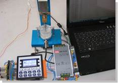 |
The packaged sensor (left) and the automated measurement platform (right) |
|
| Eco-nanotechnologies and Advanced Materials |
| Development of a SiNWs-based substrate with application in genetic analysis |
Competency:
Smart specialization: |
NANO MAT: Advanced materials and nanotechnologies
Eco-nanotechnologies and Advanced Materials |
| |
TRL 3 research to prove feasibility / Analytical and experimental critical function proof of concept
Contact Person: Monica Simion ([email protected]); Melania Banu ([email protected]) |
| |
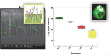
The feasibility of a novel microarray support based on silicon nanowires was explored in joint effort between IMT, University of Bucharest and the laboratory of genetic analysis GeneticLab, aiming to increase the detection rate of the DNA sequence mismatches with pathological significance occurred in BRCA1 gene.
The single-base differences were detected by scanning the slides after the hybridization process carried with fluorescently labelled complementary DNA. The nano-structured platform has disclosed a statistical detection between the differences of hybridization signal intensities.
|
| Supplement National Priority: Health (including medicine industry) |
| Microfluidic biochip for Melanoma cells study |
Competency:
Smart specialization: |
MEMS: Micro electro mechanical systems (MEMS), micro traducers, micro and nanofluidics
Health
(including medicine industry) |
| |
TRL Level: TRL 4 – technology validated in lab
Contact Person: Dr. Marioara Avram ([email protected]) |
| |
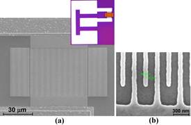
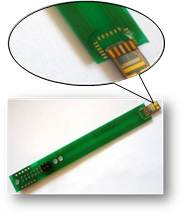
The core of microfluidic biochip is the impedance biosensor consists of two interdigitated microelectrodes, each having 64 digits, a reference electrode and a counter electrode. Using this device we have set the electrochemical impedance spectra thus deducing the dielectric properties of melanoma tumour cells: the capacitance of the double electric layer, charge transfer resistance, Warburg diffusion impedance, Nyquist diagram of dielectric permittivity, tumour cell polarization properties and the variation of the Clausius-Mossotti relation, using redox species.
The microfluidic biochip is designed to fit into an USB port, having the sensing chamber of 2x1mm2. Both the microelectrode finger width and spacing are 5 μm. The reference and the counter electrode width is 100 μm and 300 μm, respectively. The reaction chamber contains 64 pairs of interdigitated microelectrodes, a counter electrode, and the reference electrode. Fluidic microchannels were designed to minimize interaction between biochemical reactive, while maximizing the detection and analysis selectivity. Seven independent microchannels are attributed to a specific testing solution depending on their injection succession. The microchannel for the fluid to enter last during the analysis has the shortest path to the reaction chamber. Each microchannel is 150 μm wide and 100 μm deep.
 |
(a). Design of one biochip; (b). Reaction chamber
(c). Dielectrophoretic device (1 cm width and 2 cm length) in an USB port with detail on the reaction chamber. |
|
| Reagent based on gold nanoparticles for mapping of tumor tissue architecture |
Competency:
Smart specialization: |
NANO MAT: Advanced materials and nanotechnologies
Health (including medicine industry) |
| |
TRL 3 research to prove feasibility / Analytical and experimental critical function proof of concept
Contact Person: Dr. Marioara Avram ([email protected]) |
| |
The new method refers to the preparation procedure of a reagent based on colloidal gold and its use for tissue mapping, the purpose being to determine tumor limits both on the surface and in depth, including the emphasis of the tumor cell nests in the proximity of the tumor. The tissue mapping was done by fluorescence microscopy with two laser beams (with 450 nm and 570 nm wavelengths), and was possible due to the emission in a fluorescent spectrum of the gold nanoparticles. This imagistic effect can be explained theoretically by Localized Surface Plasmonic Resonance (LSPR) at the interface between the gold nanoparticles and the dielectric environment in which they are immersed, the light intensity of the plasmons being all the stronger, as long as the refraction index of the environment where the nanoparticles have been transported by endocytosis is larger and, implicitly, the dielectric permittivity of the environment is larger.
The technical problem set forth to be solved is the mapping of the tumor tissue architecture in order to determine the edges of the tumor both on the surface and in depth. In order to solve this problem, plasmonic resonance through gold nanoparticles with an average diameter of 5.6 nm, was studied experimentally by inducing it in the tumor tissue B16 melanoma of mice, which resembles most the type of cutaneous melanoma found in humans. The main purpose of the experiments was the histopathological investigation of the tumor tissue in UV light with an excitation wavelength of 450 nm, after the administration of gold nanoparticles suspended in sodium citrate solution.
The method has the advantage that it proposes a non-toxic, easily obtainable reagent, which is efficient in utilizing it in a safe method of analysis, both of the tumor and its surroundings, but also of the tumor roots in the healthy tissue. |