|
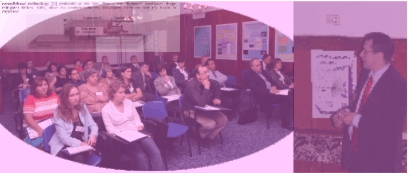
Invited Speakers CAS 2012
 |
Dr. Rens Baggen graduated from the Technical University of Eindhoven in 1992 (ir.) with emphasis on antennas and propagation, and started working at the Dutch Aerospace Laboratory (NLR) in Amsterdam in 1993. There he worked in the fields of avionics and quality management.
In 1995 he joined the department of Antennas & EMC of the IMST and specialised in antenna theory, simulation methods and tools, waveguide antennas, metamaterials and measurement techniques, amongst others. Phased array technology is one of his main topics.
His work involves also management and acquisition and coordination/management of long term EU- and European Space Agency-projects. |
 |
Prof. José Millán received the B. Sc. Degree from the University of Navarra (1971) and a Ph.D. in Electronics with honors from the Autonomous University of Barcelona (UAB) in 1980. He has been Assistant Professor at the UAB (1980-1987). In 1987 he joined CNM. He got the grade of Full Professor of CSIC in 1991 and Deputy-Director of CNM-Barcelona (Feb 1999-Feb 2003 and March 2006-June 2008). His research activity is related to process technologies (Si and WBG semiconductors) for power devices and microsystems. He has published more than 290 papers including regular and international conference papers. He has participated in 32 national projects, 22 European projects and 21 industrial contracts. He also holds 12 patents. |
 |
Liviu NICU was born in 1973 in Bucharest (Romania). After completing his Master of Electrical Engineering at the Paul Sabatier University of Toulouse (France) in 1997, he joined the Integrated Microsystems Group at the LAAS (Laboratory for Analysis and Architecture of Systems) of Toulouse where he obtained his PhD in 2000 into the Micromechanical Structures field. From 2000 to 2003, he was R&D Engineer at Thales Avionics, Valence (France). His activities focused onto the development of micromechanical sensors for the civil and military navigation applications. Since 2008 he is leading the NanoBioSystems Group at LAAS as a full time CNRS (National Center of Scientific Research) researcher where he currently works in two main research fields: the development of (1) new resonant bio(chemical)sensors using M(N)EMS technologies and of (2) cantilever-based microsystems for contact deposition of small amounts of biological samples for biochip applications. |
 |
Dr. Stefano Bellucci, obtained in 1986 his Ph.D. in Physics of elementary particles at SISSA, Trieste, Italy. He worked as a Research Associate at Brandeis Univ., Waltham, MA, USA (1983-1985); as a visiting researcher at M.I.T., Cambridge, MA, USA (1985-1986); as a visiting researcher at the Univ. of Maryland, USA (1986-1987); as a visiting researcher at the Univ. of California at Davis, USA (1987-1988). He was appointed as a Tenured Researcher (Research Staff) at INFN (Istituto Nazionale di Fisica Nucleare) Laboratori Nazionali di Frascati in 1987. He was appointed as a First Researcher (Senior Research Staff), at the same Institute in 2005. He currently coordinates all theoretical physics activities at his Institution in Frascati. His research interests include theoretical physics, condensed matter, nanoscience and nanotechnology, nanocarbon based composites, biomedical applications. His lab has cultivated more than 10 between PhD students and master students in the fields of theoretical physics, condensed matter, nanoscience and nanotechnology. His scientific contributions to the community include (i) supersymmetric mechanics, (ii) black holes in supergravity, (iii) toxicity of nanomaterials, (iv) pion polarizabilities, (v) gravitational waves. He has published over 300 papers in peer-reviewed journals (with h = 34), and more than 10 invited book chapters. He is the Editor of 8 books with Springer. He appears in the list of Top Italian Scientists published by the VIA Academy.
Dr. Bellucci was the recipient of the B.W. Lee Prize at the Erice School of Subnuclear Physics (Erice, Italy) 1982. In 1980 he was selected as a Summer student at CERN (Geneva).
Dr. Bellucci serves both as the Series Editor of the Springer Lecture Notes in Nanoscale Science and Technology, and the Associate Editor of Nanoscience and Nanotechnology Letters. He is, as well as, the Editorial Board Member of the following scientific journals:
- Physics International
- Computer Modelling & New Technologies, ISSN 1407-5806
- Journal of Materials - the Global Journal of Physics Express
- The Journal of Physics & Astronomy.
He currently carries responsibilities within the following European and Italian national projects:
- INFN scientist in charge of the EU project BY-NanoERA—Institutional Development of Applied Nanoelectromagnetics: Belarus in ERA Widening
- INFN scientist in charge of the EU project FAEMCAR—Fundamental and Applied Electromagnetics of Nano-Carbons
- INFN scientist in charge of the Italian Research Ministry PRIN project DENSE on nanocomposites
- LNF Spokesperson of MI12 Supersymmetry project CSN-4
- National Spokesperson of LF61 Condensed Matter Theory project CSN-4.
Dr. Bellucci is European Commission Expert for the Research Framework Programmes. He is also Italian Research Ministry Expert in Industrial Research - D.Lgs. 297/1999. |
 |
Acad. Ion Tiginyanu received his M.S. degree from the Moscow Institute of Physics and Engineering in 1978. He received his Ph.D. degree in Physics from Lebedev Institute of Physics, Academy of Sciences of U.S.S.R. From 1984 to 1998 he worked as senior researcher at the Institute of Applied Physics of the Academy of Sciences of Moldova. In 1998 he joined the Technical University of Moldova, being appointed vice-Rector, while in October 2004 he was elected vice-president of the Academy of Sciences of Moldova. He serves as Director of the National Center for Materials Study and Testing. In 1995-96 he has been a visiting professor at the Technical University Darmstadt, Germany, while in 2001 - at the University of Michigan, USA. Professor Tiginyanu’s research interests are related to nanotechnologies, metamaterials, ultrathin membranes, optical phonon engineering, random lasing, THz emitters, new solar cell and sensor technologies. He has more than 250 journal papers and 50 technological patents, his personal Hirsch factor equals 25. He is a member of AAAS, IEEE, OSA, SPIE, MRS and Electrochemical Society. More information on his research can be found at http://www.ncmst.utm.md. |
 |
DI (FH) Roland Staudinger is Regional Sales Manager at EV Group Europe & Asia Pacific GmbH, responsible for the territory of the Eastern and South Eastern part of Europe. He is with EVG since beginning of 2003 and after various positions like Key Account Project Management he joined the Sales team in 2010. He graduated at the University of Applied Sciences Upper Austria for Mechatronics and Economics with the focus on Robotics and Automation. The topic of the diploma thesis was related to special thin wafer handling with electrostatic force. Prior to his career at EVG he was working as Product Manager for Wireless solutions in the computer industry, realizing innovative projects in an international environment. |
 |
Friedhelm D. Bauer received the M.S and Ph.D. degrees in electrical engineering from Rheinisch Westfälische Technische Hochschule (RWTH) Aachen, Germany, in 1979 and 1984, respectively.
From 1986 to the present, he has been involved in the research and development of high-voltage high-power semiconductor switches such as MOS-controlled thyristors, IGCTs and IGBTs at ABB Corporate Research, Switzerland, and later at ABB Semiconductors AG, Lenzburg, Switzerland. Since 2004, he has been a Senior Principal Scientist with the Corporate Research Center, ABB Switzerland Ltd., Baden-Dättwil, Switzerland. He is the author of a number of scientific papers in the field of modern power semiconductor devices. He is also the holder of several patents in the same field. |
 |
Claudiu V. Falub obtained his PhD in natural sciences from the Delft University of Technology (TU-Delft), The Netherlands, in 2002. His major fields of study were positrontwo-dimensional angular-correlation-of-annihilation-radiation (2D-ACAR) of thin films, nanocavities and quantum dots, using a unique in the world reactor-based facility built during his PhD project. He was a post-doctoral associate at the Paul Scherrer Institute (PSI), Switzerland, from 2002 to 2005, where he was responsible within two EU projects (SiGeNET, SHINE) for the molecular beam epitaxy and the synchrotron radiation high-resolution X-ray scattering of complex quantum cascade structures based on group-IV semiconductors. Between 2005 and 2010 he was a scientific collaborator and a research associate at the Swiss Federal Institute of Technology Lausanne (EPFL), and the Swiss Federal Laboratories for Materials Science and Technology (Empa), where he collaborated with several global players in the field of high-tech coatings for precision tools and biomedical implants. Since 2010, he has been a senior scientist at the Swiss Federal Institute of Technology Zürich (ETHZ), where he works on the development of a new kind of X-ray imaging detector based on germanium absorbing layers. In collaboration with researchers from the Milan Polytechnic, University of Milan-Bicocca and the Swiss Center for Electronics and Microtechnology (CSEM), he has recently achieved a major breakthrough in semiconductor technology, which solves the decades-old problems of crystal defects, layer cracks and wafer bowing. He has authored or co-authored more than 50 peer-review scientific publications, including a cover story of the Science magazine, and has one patent application. |
 |
Dr. Syed Zeeshan Ali is a Senior R&D Engineer at Cambridge CMOS Sensors Ltd in UK. He graduated from GIK Institute, Pakistan in Electronic Engineering. He completed his Phd at the University of Cambridge researching on micro-hotplates for gas sensors. Afterwards he continued as a research associate at the university researching on micro-gas sensor before joining Cambridge CMOS Sensors, a spin-off company from Cambridge University. Dr. Ali's research interests are on SOI membrane devices for micro-sensors including gas, flow and temperature sensors. His work includes electro-thermal and mechanical analysis of sensors as well as sensors for high temperatures. |
|