PHOTONTECH
|
| Home | |
| Partners | |
| Objectives | |
| Resources | |
| Activities/Results | |
| Publications | |
| Related EU Projects | |
| Events | |
| Contact |
FINAL project - Processing of SOI (silicon-on insulator) wafers for microphotonics [...]
- Thin film technologies [...]
- Multilayer structures with controlled optical properties [...]
- Laser direct processing [...]
- Modeling/simulation of advanced materials and structures [...]
- Integration of mixed processes and experimentation of demonstrative photonic microstructure [...]
- Dissemination and Education [...]
- European projects (FP7) [...]1. Processing of SOI (silicon-on insulator) wafers for microphotonics
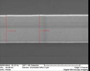
We experimented and optimized techniques for fabrication of microphotonic structures (mirrors, cantilevers, optical waveguides) on SOI wafers. We optimized Silicon dry etching (reactive ion etching) using a new equipment and SiO2 wet etching to obtain free standing microstructures on SOI wafers.
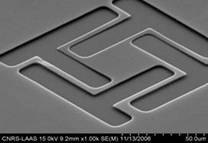
Fig. 1. SEM images of photonic microstructures obtained on SOI wafers: a) Movable micro-mirror for “free space interconnections”; b) Si waveguide for optical communications2. Thin film technologies
2.1. Polymer technology
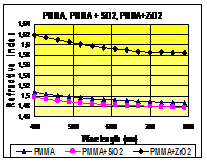
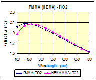
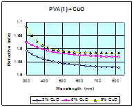
Polymer nanocomposites for photonics applications, with controlled refractive index in the range 1.46-1.78 were prepared by chemical route and sol-gel process, starting from polymethylmethacrylate (PMMA), hydroxyethylmethacrylate (HEMA), polyvinilic alcohol (PVA) and metal oxides from alcoxides or inorganic compounds. The properties of these materials, modified by metal oxide nanoparticles depend on the composition/metal oxide concentration, particle size and dispersion homogeneity. Ellipsometric method was used to analyse the changes in the refractive index of the nanocomposites with respect to increasing particle concentration and the spectrophotometry to determine the optical transmittance. The size and dispersity of the nanoparticles in the polymer matrix were appreciated with scanning electron microscopy (SEM) and atomic force microscopy (AFM). As expected, the refractive index measured on the polymer thin films spin coated onto substrates increases with respect to oxide concentration for the polymers modified with TiO2, ZrO2 or CuO in the entire visible region and decreases with the oxide concentration when the polymers are modified with SiO2 (fig.2). For the all compound the transmittance remains above 90% in the visible wavelength spectra. The particle dimensions are in the range 10 - 70 nm and were controlled through the parameters and the method of synthesis.
The experiments showed that the refractive index of the polymers can be adjusted in the range 1.45-1.78 by controlling the nature and the concentration of the metal oxides incorporated in polymer solutions. The doped polymer solutions can be easily spin-coated and the coatings combine the optical transmittance of polymer with the high refractive index of the metal oxide mixed into polymer solution. This method is simple, inexpensive and the doped polymer can be used in photonic applications (example- fig. 3).
Fig. 2. Refractive index spectra of polymers doped with metal oxides.

Fig. 3 Images of PMMA rib waveguides with V-shape
2.2. Sol-gel technologies
The multilayer titania and silica-titania waveguides undoped and doped with Er3+ were prepared by sol-gel method. The sol-gel method is a flexible and convenient way to prepare oxide films on several types of substrates, and for this reasons it was extensively investigated for optical waveguides fabrication. The selected molar composition was 100% TiO2 for high refractive index and 90%SiO2-10%TiO2 for the Er doped layers. The films were deposited on Si/SiO2 substrate by dip coating and by spin coating methods, followed by annealing at 3000C (TiO2 based layers) or 9000C for the SiO2-TiO2-Er system.
The films were characterized by SE in the range of 300-700 nm, by fluorescence and IR spectroscopy, as well as by AFM and SEM. Continuous and homogeneous films with a good adherence to the substrate have been obtained by sol-gel method, alkoxide route by the two methods of deposition: dip and spin coating. The spectro-ellipsometric results show a densification of the film with the temperature of thermal treatment; this means a decrease in thickness and an increase in refractive index. The thickness of multilayer film grows linearly with the film numbers. The SiO2-TiO2-Er system presents fluorescence spectra starting with 4 layer deposition.
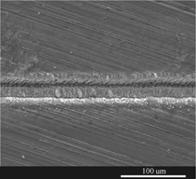
Optical waveguides and photonic circuits (microring resonators) were obtained by patterning Er-doped SiO2-TiO2 sol-gel layers deposited on oxidized silicon wafers (oxide thickness over 1700nm). Two techniques were used for patterning: wet etching in buffered oxide etch (BOE) solution (40% NH4F : 49% HF = 6:1) with an etching rate 120 nm/min at 22oC and reactive ion etching in CF4 (max. etching rate: 80nm/min – at 250 W). Reactive ion etching offers a better control of the etching process and lower over-etching.

Fig. 4. a) SEM image of a TiO2 ring resonator; b) IR image of an SiO2-TiO2-Er –based waveguide ( light propagation l – 1550 nm).3. Multilayer structures with controlled optical properties
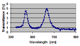
We have obtained thin layers of dielectrics and metallic materials with adequate properties for selective detection of optical radiation. Multilayered functional structure from SiO2, TiO2, Ag, Al thin layers has been obtain with a selective response. The metallic layers have been obtained semitransparent with a thickness in the range 20-40nm and the dielectric films have 300-500nm. The single layers have been characterized regarding optical properties by photometric and spectroelipsometric measurements and morphological properties by AFM techniques. The process parameters have been rigorously controlled in order to obtain the thickness and refractive index as simulations have indicated in order to achieve multilayers structures with selective spectral response.
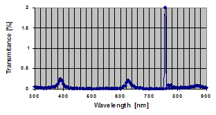
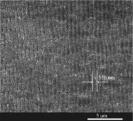
Fig.5. Spectral transmitance of multilayer optical filters, Al/ SiO2 /Ag with different dielectric thickness.4. Laser direct processing via surface ablation using a set-up with femtosecond laser system developed by INFLPR. The system can be used to pattern glass, silicon, polymers and metals.
a) b)
Fig. 6. SEM images of the patterned structures: a) structures with feature size 550 nm (pulse energy 15 nJ, speed 2 mm/s; b) U groove for optical fibre positioning (energy10 nJ, scanning speed 0.1 mm/s, 10 times).5. Modeling/simulation of advanced materials and structures
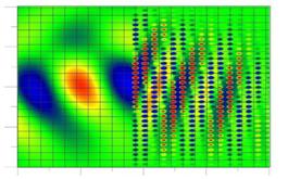
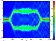
New modeling and simulation techniques for photonic circuits and metamaterials were developed using commercial software (OptiFDTD, OptiBPM, Optigrating from Optiwave-Canada) and home made software.
a) b)
Fig. 7. a) Field distribution in a Mach Zender Interferometer; b) Negative refraction in a structure presenting LHM properties (FDTD analysis)6. Integration of mixed processes and experimentation of demonstrative photonic microstructure
The developed processes were optimized and integrated to obtain new complex structures.6.1. Microsytem for optical interconnects composed of PMMA waveguides fabricated by deep-UV induced refractive index modification integrated with the silicon photodiodes. A polyimide layer was used to improve the adhesion of the PMMA layer to the silicon wafer. The end phase of the waveguide was patterned by lithography methods to obtain low fibre to chip coupling loss. The propagation loss of the waveguides was 0.16 dB/cm at 650 nm. The fibre to chip coupling loss was 1.2-2.7 dB/facet depending on the dicing quality. Over the active area of the photodiode, this layer is removed to allow a gradually transfer of the optical power from the waveguide into the photodiode by leaky wave coupling A controlled degree of coupling within a reasonable coupling length can be achieved with a tapered geometry. If the coupling length is short enough, most of the optical power remains in the waveguide and the waveguide can be coupled with other photodiodes thus the two photodiodes are optically interconnected. In our experiments, 47% of the optical power was transferred into the photodiode within a coupling length of 200mm.

Fig. 8. Optical coupling of two photodiodes via a PMA waveguide.
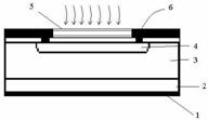
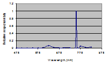
6.2. Photodetector with selective spectral response was fabricated by integration of a thin films optical filter of Fabry – Perot type with a silicon PIN photodiode with an active area of 0.6mm2 fabricated by silicon planar technology. After completion of the photodiode fabrication process the formation of multilayer optical filter starts with the deposition of a 20nm Al layer on top of the photodiode. The thin Al layer is deposited and patterned using a lift-off process. Subsequently, the dielectric layer of SiO2 with a thickness of 475nm is deposited by vacuum thermal evaporation technique. For another wavelength the thickness of the dielectric layer is thinned by plasma etching process. A silver layer of 45nm at the very end of fabrication process is deposited and patterned by lift-off. The thickness of the dielectric layer enclosed between the two semitransparent metallic mirrors determines the wavelength which will be transmitted.
a) b) c)
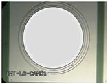
Fig. 9. a) Schematic structure of the photodetector with selective spectral response: 1-backside metallization; 2- N+ silicon substrate; 3- N silicon epitaxial layer; 4- P+ diffused region; 5-optical filter; 6-front side electrical contact. b) Optical microscope image of the structure. c) Spectral response of the structure.7. Dissemination and Education
The results of the project were presented in 7 books, 18 journal papers and more than 50 papers for international conferences
IMT and CCO organized a master program in Optoelectronics and UAIC a master program in Thin Films.
Undergraduate and PhD students have been involved in the research activity and trained in design/simulation, characterization and processing of microphotonic devices8. European projects (FP7)
IMT coordinates the FP7 project MIMOMEMS (European Centre of Excellence in Microwave, Millimetre Wave and Optical Devices, based on Micro-Electro-Mechanical Systems for Advanced Communication Systems and Sensors), Grant agreement no.:202897 (2008-2011), program Capacities