GRAPHENEFERRO
Advanced nanoelectronic devices based on graphene/ferroelectric heterostructures
(Dispozitive nanoelectronice avansate bazate pe heterostructuri grafena/feroelectric)
|
|
 |
Financed by:
|
|
| Back |
|
|
| |
|
|
| ¤ Results 2022 [...] |
|
¤ Results 2020 [...] |
| ¤ Results 2021 [...] |
|
¤ Results 2019 [...] |
| |
|
¤ Results 2018 (August-December 2018) [...] |
| |
|
|
| ¤ Results 2022 |
| |
Grapheneferro 2022 results
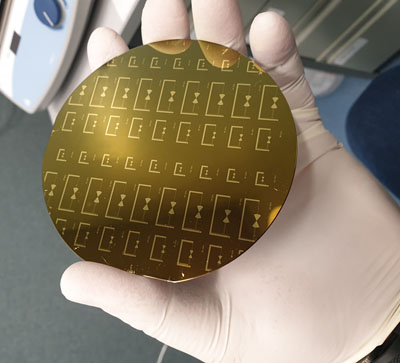
In the first six months of 2022 the last stage of this project was accomplished by buildiding a demonstrator based on the thermoelectricity of graphene/ferroelectric heterostructures.cTwo types of devices were fabricated and tested. The ferroelectric was HfZrO and the demonstrator was fabricated on 4 inch wafer scale. Two types of devices were fabricated and tested.
1.FET with nonuniform graphene monolayers channels having the shape of Greek letter Δ and bowtie since it known that such non-uniform shapes enhances the thermoelectric properties ( see for example ] A. Harzheim, J. Spiece, C. Evangeli, E. McCann,V. Falko, Y. Sheng, J. H. Warner, G. Andrew, D. Briggs, J. A. Mol, P. Gehring, O. V. Kolosov, Geometrically enhancred thermoelectric effects in graphene nanoconstrictions, Nano Lett. 18, 7719-7725 (2018).
In Fig. 1 the SEM images of these FETs are presented.
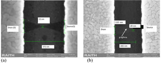 |
| Fig. 1 (a) SEM image of (a) graphene FET with bowtie channel shape (b) graphene FET with delta channel shape. |
The measurements were performed in the range 200C-600C ,using Keithley 4200 equipped with an external heater (see Fig.2).
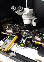 |
| Fig.2 the setup for the measurement of the graphene FETs with nonuniform channels |
The maximum Seebeck coefficient was found to be 15 µV/K for FETs having graphene channel shaped as Greek delta letter and 200 µV/K for the FETs having graphene channel shaped as a bowtie. More results will be available here after the publication of this work.
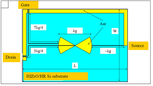
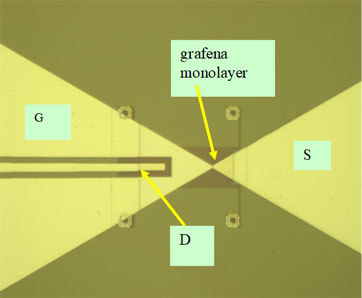
The second circuit was a microwave transistor where the gate is the hot electrode and massive source is the cold electrode (see for example [5]M.R.Gasper,R.C.Toonen, N.C.Varaljay, R.R. Romanofsky, F.A. Miranda, Thermoelectric graphene nanoconstrictions as detector of microwave signals, IEEE Trans. Nanotechnology 18, 879-884 (2019). In Fig. 3a we present the SEM image of this transistor having as channel graphene monolayer grown on HfZrO and in Fig. 3b , the optical image of this FET fabricated on a 4 inch scale.
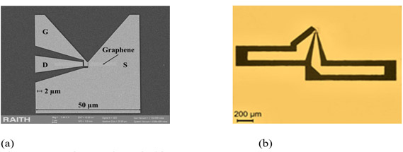 |
| Fig.3 (a) SEM image (b) optical image |
The measurement system of thermoelectric properties is displayed in Fig.4.
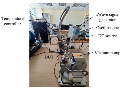 |
| Fig. 4 The setup for the microwave thermoelectric FET |
The thermoelectric signal is measured by pumping microwaves at different powers in the range 0.1-10.5 GHz , the drain bias being 0V. The result is displayed in Fig. 5
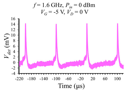 |
| Fig. 5 The thermoelectric signal at 1.6 GHz. |
More results will be available after the publication of these results.
|
| ¤ Results 2021 |
| |
In 2021 we have focused on the development of the ferroelctrics at the wafer scale and two demonstrators.
1. We have developed at the wafer scale a new ferroelectric based on HfO2 which is obtained by doping HfO2 with Ge nanoparticles (HfGeO).
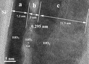
In Fig.1 we see the HRTEM structure of of 3 layers stack: HfO2 orthorhombic/tetragonal phase (0.295 nm lattice fringe) in the intermediate layer (HfO2 + Ge).
| Fig. 1 HRTEM image of the ferroelectric HfO2 film of 3 layers stack: HfO2 orthorhombic/tetragonal phase (0.295 nm lattice fringe) in the intermediate layer (HfO2 + Ge) [1] |
In Fig. 2, we have presented the P(E) of HGeO in different situations.
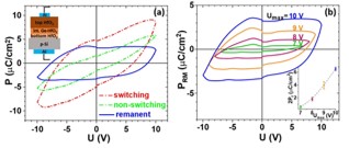 |
Fig. 2 P(E) of HfGeO |
Many other structural characterization were performed .
The PZT was developed on 4 inch Si wafers as it is shown in Fig. 3.
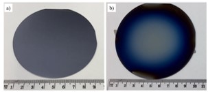 |
Fig. 3 PZT wafers on Si |
Using HfGeO we have developed the two demonstrators of the project
1. Logic circuits based on graphene/ferroelectric heterostructures.
The cross-section of the device is presented in Fig. 4
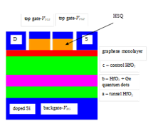 |
Fig. 4 Reconfigurable logic gates based on graphene/HfGeO FETs |
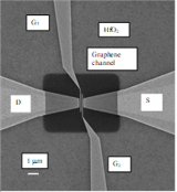
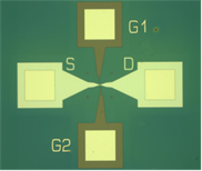
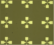
We have designed and fabricated an array of 225 field-effects- transistors (FETs) having graphene monolayer channels. The graphene was transferred at the wafer scale on the heterostructure of 22 nm control HfO2/5 nm Ge-doped HfO2 intermediate layer/8 nm tunnel HfO2/p-Si substrate. The intermediate layer of Ge-doped HfO2 (HfGeO) is ferroelectric and acts as floating gates, the structural and electrical properties of (HfGeO) being presented in [32]. These transistors have two top gates, whereas the bottom substrate, which is p-Si, is a back gate. These FETs work as a two-input reconfigurable logic gates with memory, various logic gates can be programmed using the two top-gate voltages or a top-gate voltage and the back-gate voltage. The SEM image of the FET is represented in Fig.5, while its optical image is represented in Fig. 6 and part of the array in Fig.7
The three-gates are programmed with the following gate voltages: +4 V, -4 V, and 0 V while the output is the drain current where its output logical 0 state is assigned for the case when all gates are 0V. In this way, OR gates and NAND gates are realised.
2. Neuromorphic demonstrator is a memtransistor based on HfGeOwhich is an artifical synapse transistor (more details in [1]).
We have obtained experimental results regarding a FET with graphene monolayer channel transferred over the ferroelectric structure HfO2/Ge-HfO2 / HfO2, which behaves as a memtransistor-like structure and works at very low drain voltages compared with the above devices, i.e. in the range of -2 to +2 V, while the gate voltages are of few volts, the transistor being off at a gate voltage of 9 V. In this respect, we have combined two principles leading to synaptic transistors mentioned above, i.e. the ferroelectricity and floating gate in a single device. Since all memtransistors reported up to now are using flakes of MoS2, we have radically changed the materials and technologies in order to fabricate the devices at the wafer scale. We have chosen the configuration of 3-layers-stack consisting of control HfO2/Ge-HfO2 intermediate layer/tunnel HfO2/p-Si substrate with ferroelectric properties. This 3-layers-configuration has the advantage of obtaining orthorhombic HfO2 phase by employing both strain and doping induced by Ge and is deposited on 3x3 cm2 doped Si substrate, its top layer being covered with graphene monolayer transferred by Graphenea. The schematic cross-section of the memtransistor is depicted in Fig. 8. It is a FET having a top and a back gate, its graphene monolayer channel being isolated from the top gate electrode by HSQ (Hydrogen silsesquioxane). Tens of FETs were fabricated on the same wafer.
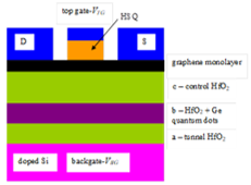 |
Fig. 8 The memtransistor configuration. |
 |
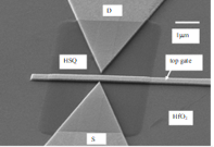 |
Fig. 9 The optical image of the memtransistor graphene/HfGeO. |
Fig.10 The SEM photo of the memtransistor. |
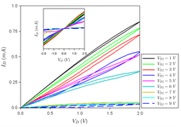
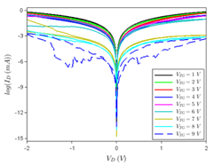
The  versus positive drain voltage versus positive drain voltage  at various top gate voltages. Inset : at various top gate voltages. Inset :  - - for drain voltages in the range -2 to +2 V are displayed in Fig. 11 for drain voltages in the range -2 to +2 V are displayed in Fig. 11
In Fig.12 the drain current dependence in time for a drain voltage of +2 V (top) and -2 V (bottom).We see that the conductance of the memtransistors is increasing/decreasing in time as in the case of the synapses.
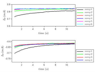 |
Fig. 12 the drain current in time when drain voltage of ± 2V are applied. |
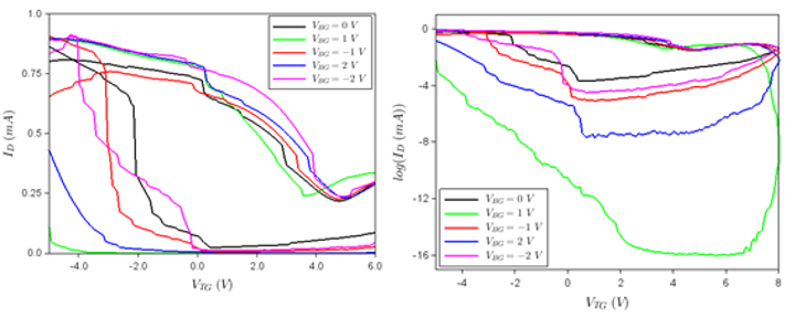
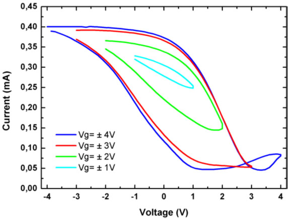
The transistor is acting as a memtransitor with a high on/off ratio. Both top and back gates are controlling the flow of carriers in the graphene channel even at small values, of few volts. The top gate is driving the transistor in on/off states with hysteretic behaviour while the backgate voltage controls the current flow/drain current in graphene, modulating the on/off ratio depending on its polarity, as in the case of a memristor. The transistor is a non-volatile memory since its  versus positive drain voltage versus positive drain voltage  and and  versus top gate voltage versus top gate voltage  for different backgate voltages for different backgate voltages  (see Fig. 13) show a hysteretic behaviour. (see Fig. 13) show a hysteretic behaviour.
The next stage of the project is to investigate thermoelectric properties of the graphene/ferroelectric structures.
References
- M.Dragoman, A.Dinescu, D. Dragoman, C. Palade, A. Moldovan, M. Dinescu, V.S. Teodorescu, M.L. Ciurea, Wafer-Scale graphene-ferroelectric HfO2/Ge-HfO2/ HfO2 transistors acting as three-terminal memristors, Nanotechnology, , 31 495207 (2020).
Papers published by the consortium in 2021.
Journals
- M. Dragoman , M. Aldrigo, D. Dragoman, Perspectives on atomic-scale Switches for high-frequency applications based on nanomaterials, Nanomaterials 11, 625 (2021).
- M. Dragoman , A. Dinescu, D. Dragoman and F. Comanescu, Bloch oscillations at room temperature in graphene/h-BN electrostatic superlattices, Nanotechnology 32, 345203 (2021).
- M. Aldrigo, M.Dragoman, S. Iordanescu, A.Avram, O-G Simionescu, C.Parvulescu, H. El Ghannudi, S. Montori, L.Nicchi, S.Xavier and A. Ziaei, Tunable 24-GHz Antenna arrays based on nanocrystalline graphite, IEEE Access 9, 122443- 122456 (2021).
- M. Dragoman, M. Aldrigo, D. Dragoman, S. Iordanescu A. Dinescu, and M. Modreanu, HfO2-based ferroelectrics applications in nanoelectronics, Phys. Status Solidi RRL 2000521(2021).
- M. Dragoman , M. Aldrigo , D. Dragoman , Ian M. Povey S. Iordanescu , A. Dinescu , A. Di Donato , M. Modreanu, Multifunctionalities of 2D MoS2 self-switching diode as memristor and photodetector, Physica E 126 114451 (2021).
- M. Dragoman, Martino Aldrigo, Daniela Dragoman, S. Iordanescu, A. Dinescu, M. Modreanu , The rise of ferroelectricity at nanoscale, Nanotechnology Magazine, vol. 15, , pp. 8-19, (2021).
- I. Stavarache , O.Cojocaru, V. A. Maraloiu , V.S. Teodorescu , T. Stoica , M. L. Ciurea, Effects of Ge-related storage centers formation in Al2O3 enhancing the performance of floating gate memories , Appl.Surf.Sci 542 148702 (2021).
- C.Palade, A.-M. Lepadatu, A. Slav, O. Cojocaru, A. Iuga, V. A. Maraloiu, A. Moldovan, M. Dinescu, V. S. Teodorescu, T. Stoica ,M. L. Ciurea, A nanoscale continuous transition from the monoclinic to ferroelectric orthorhombic phase inside HfO2 nanocrystals stabilized by HfO2 capping and self-controlled Ge doping, Journal of Materials Chemistry C, 9, 12353–12366(2021)
Conferences
- M. Dragoman , D. Dragoman , A. Dinescu, Novel functional materials: 2D materials/ferroelectric heterostructures for nanoelectronics, EMRS Spring Meeting, 2021- Symposium N.VI.4- invited paper
- M. Dragoman, M. Aldrigo, D. Dragoman, S. Iordanescu, A. Dinescu, M. Modreanu ,Microwave and THz devices using HfO2-based ferroelectrics
EMRS Fall Meeting, 2021- Symposium Q1 - invited paper.
- M. Dragoman, M. Aldrigo, D. Dragoman2,3, S, Iordanescu, A. Dinescu1, F. Nastase, M. Modreanu, The rediscovery of ferroelectricity at the nanoscale , , Chisinau , ICNMBE , R. Moldova, 2021, invited paper
- M. Aldrigo, M. Dragoman, S. Iordanescu, D. Vasilache, A. Dinescu, Biagetti, L. Pierantoni, D. Mencarelli, Microwave detection using 2-Atom-thick heterojunctions, IEEE MTT Symp. 2021.
- A.M. Lepadatu, C. Palade, I. Dascalescu, A. Slav, I. Stavarache, A.V. Maraloiu, V.S. Teodorescu, T. Stoica, M.L. Ciurea, „SiGeSn quantum dots for non-volatile memories”, EMRS 2021 Fall Meeting, 20-23 septembrie 2021
- C. Palade, A.M. Lepadatu, A. Slav, O. Cojocaru, A. Iuga, V.A. Maraloiu, A. Moldovan, M. Dinescu, V.S. Teodorescu, T. Stoica, M.L. Ciurea, „Ferroelectric orthorhombic HfO2 phase in 3-layer memory structures of control HfO2 /floating gate of Ge nanoparticles in HfO2 /tunnel HfO2 on Si wafers”, Materials Challenges for Memory - MCFM 2021 (https://horizons.aip.org/materials-challenges/), virtual conference, 11-13 aprilie 2021
|
| |
|
|
| ¤ Results 2020 |
|
|
The project is oriented in 2020 for the design, fabrication and first measurements of the first demonstrator of the project -Graphene field-effect transistors (FETs) based on graphene/ferroelectric heterostructures for high-frequency applications-demo D1, which is a field-effect transistor integrated with antenna for the detection of high-frequency signals up to THz frequencies.
1. In this respect, based on the results obtained previously we have fabricated first HfO2-based ferroelectric by doping it with Zr (termed HfZrO) and Ge (termed HfGeO), and the fabrication of PZT was extended by new equipments to 3-4 inch wafers of PZT to be grown on various substrates.
-The fabrication of HfZrO by the ALD was performed on 4 inch high-resistivity Si (HR Si) substrate for demonstrator fabrication. 20 nm of Al2O3 was deposited on HR Si by ALD and then in the next step HfZrO was grown in the same equipment without removing the Si wafer from the equipment. Below, we present the PFM of the HfZrO showing the existence of a pronounced ferroelectricity at room temperature.
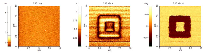
topography amplitudude PFM phase PFM
PFM for HfO2 dopedcu Zr Write on 5 µm × 5 µm, 10V ; write on pe 2 µm × 2 µm, -10V ; Read on 10 µm × 10 µm, 3V AC
-magnetron sputtering
The structure grown by magnetron sputtering is presented below:
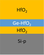 |
- HfO2 buffer: 45 W rf, thickness d = 10 nm;
- Ge-HfO2: HfO2 35 W rf, Ge 20 W dc thickness d = 10 nm;
- HfO2 45 W rf, thickness d = 20 nm; |
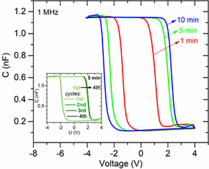
Polarization, PFM and capacitance measurements were used to characterize this HfGeO ferroelectric. Below is presented the capacitance measurements where a large memory window is observed.
PZT grown by PLD
Below we present the upgrade of PLD able to grow PZT up to 10 cm wafers implemented in 2020.
First results:
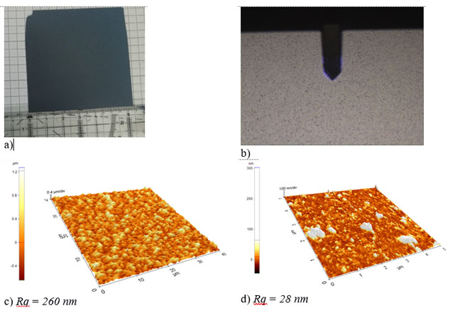
Imagini optice a) PZT wafer 6.5 x6.5 cm, b) surface of PZT (~ 480 μm x 360 μm) sAFM images 1 c) 40 µm × 40 µm, d) 5 µm × 5 µm
In all the cases the graphene monolayer was transferred by Graphenea.
The demonstrator was first designed and simulated on a 3D electromagnetic simulator and the design is presented below:
The relation between various frequencies and the dimensions of the detector is presented below:
| Frequency |
λg |
L |
W |
| 24 GHz |
4,62 mm |
14,5 mm |
~10 mm |
| 38 GHz |
2,61 mm |
8,7 mm |
8,42 mm |
| 60 GHz |
1,76 mm |
5 mm |
4,64 mm |
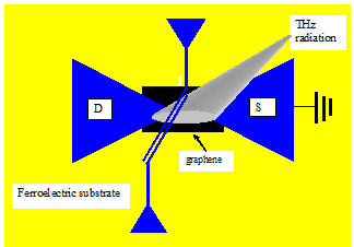
The demonstrator is a detector based on a graphene/ ferroelectric FET in copalaner waveguide technique where the gate and the drain electrodes are formed by a splitting-gate bow tie antenna.
The demonstrator was fabricated at the wafer scale:
The ID-VG dependence of the FET is displayed below:
The setup to measure the demonstrator:
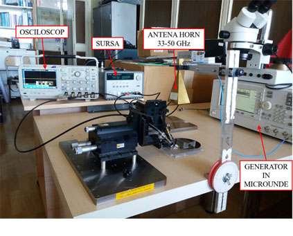
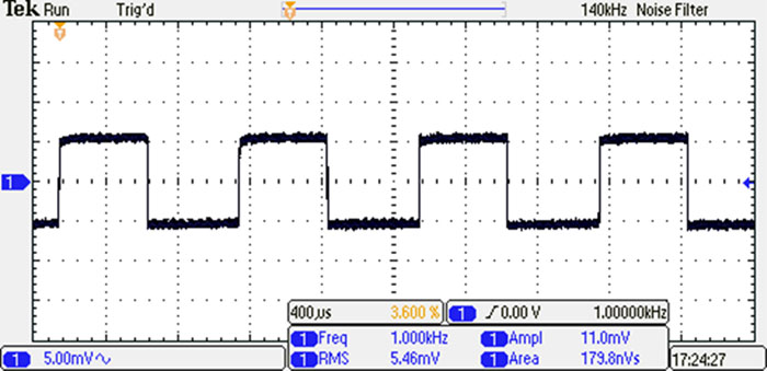
The first measurements (detection in X band- 12 GHz modulated signal with 1 kHz rectangular pulses) are presented below:
In conclusion, despite the pandemic situation which has produced considerable delay in our activities we have succeeded to accomplish all the tasks of the project and new measurements are previewed.
|
| |
¤ Results 2019
In 2019 we had the following activities :
A. We have grown HfO2-based ferroelctrics doped with Zr , Al and Ge at the wafer level on Si/SiO2 wafers and we have characterized them using XRD, PFM and microwave measurements. The majority of the results are found in the following papers:
1. S. Vulpe, F. Nastase, M. Dragoman, A. Dinescu, C. Romanitan, S. Iftimie, Antoniu Moldovan, N. Apostol, Physical properties of the ferroelectric capacitors based on
Al-doped HfO2 grown via Atomic Layer Deposition on Si, Applied Surface Science 483, 324-333 (2019 )
2. C. Palade, A. Slav, A.M. Lepadatu, I. Stavarache, I. Dascalescu, V.A. Maraloiu, C.C. Negrila, C. Logofatu, T. Stoica, V. Teodorescu, M.L. Ciurea, S. Lazanu, „Orthorhombic HfO2 with embedded Ge nanoparticles in nonvolatile memories used for the detection of ionizing radiation”, Nanotechnology 30, 365604 (2019)
3. M. Aldrigo, M.Dragoman, S. Ioradanescu, F.Nastase, S. Vulpe, A.Dinescu, and D.Vasilache, Low-voltage permittivity control of coplanar lines based on hafnium oxide ferroelectrics grown on silicon, IEEE Access 7, 136686-136686-136693 (2019).
B. We have transferred graphene on ferroelectric wafers and we have fabricated field-effect-transistors (FETs) to study their physical properties and to determine the mobility of carriers which is 8000 cm2/Vs at room temperature. We have also experimentally validated the theoretical predictions that HfZrO is opening a bandgap of 0.2 eV in graphene.
The results are found in the following papers:
1. G.A. Nemnes, D.Dragoman and M.Dragoman, Graphene bandgap induced by ferroelectric Pca21 HfO2 substrate: a first-principles study, Phys. Chem. Chem. Phys. 21, 15001-15006 (2019).
2. M. Dragoman, M. Modreanu, I. M. Povey, A. Dinescu, D. Dragoman, Reconfigurable horizontal/vertical carrier transport in graphene/HfZrO field-effect transistors, Nanotechnology 31,025203 (2020).
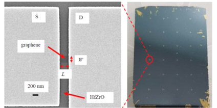
Fig. 1 Transistors on graphene/HfZrO
L=400 nm, W=300nm
C. We have designed the first demonstrator to detect high frequencies using self-switching diodes (SSD), and FETs.
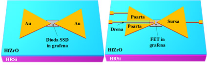
Fig.2 The demonstrator 1 : high frequency electromagnetic field detection using SSD and FETs
Some preliminary results are found in
M. Yasir, M. Aldrigo, M. Dragoman , A. Dinescu ,M. Bozzi , S. Iordanescu , D. Vasilache, Integration of antenna array and self-switching graphene diode for detection at 28 GHz, IEEE Electron Dev. Lett., 40 , 628-630 (2019).
¤ Results 2018 (August-December 2018)
We have obtained HfO2 ferroelectrics grown on Si wafer by atomic layer deposition (ALD) and magnetron sputtering by doping HfO2 with Zr. We have obtained ferroelectric PZT frown on Si by pulsed laser deposition (PLD). Also, first atomistic computation were made to study graphene/HfO2 ferroelectric interface. In this respect, we have tested tens of structures via XRD , PFM and HR-TEM and ferroelectricity was evidenced each time.Also, C-V and microwave measurements were made on tens of structures to demonstrate the ferroelectricity in HfO2 doped with Zr. The majority of the obtained results are new and will be soon published.
Keywords:graphene/ferroelectric heterostructures, nanoelectronic devices |
¤ Project coordinated by:
National Institute for Research and Development in Microtechnologies- IMT Bucharest
http://www.imt.ro/ |
 |
Partners: University of Bucharest; National Institute for Materials Physics ( NIMP) Bucharest, National Institute for Laser, Plasma & Radiation Physics (INFLPR) |
|