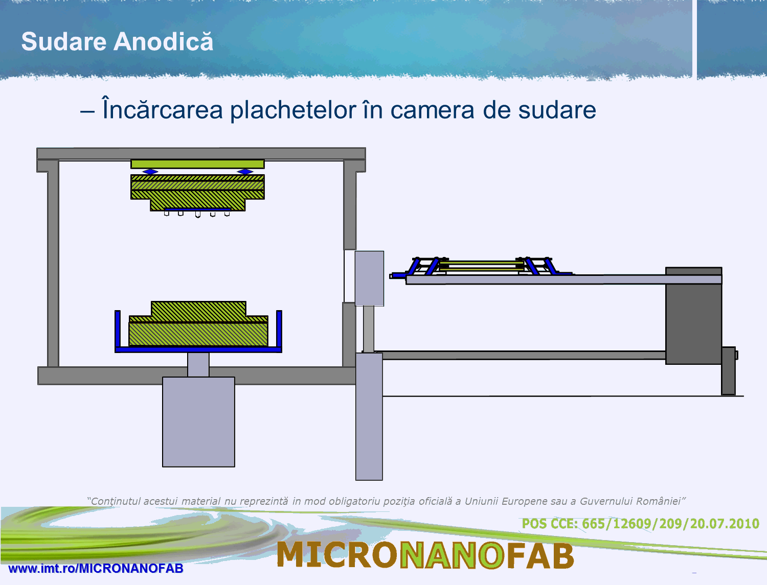
|
|
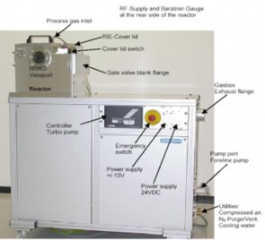
DRIE- Plasmalab System 100ICP
Deep Reactive Ion Etching System |
Reactive Ion Etching (RIE) Plasma Etcher- Etchlab 200 |
|
|
|
|
Micro PIV -PIV for Microfluidics
(Particle Image Velocimetry) |
Wafer Bonder System- SB6L-
Wafer -
Substrate Bonder System |
| |
|
|
Refractometer for layer thickness measurements - NanoCalc-XR |
| |
|
| |
| |
| |
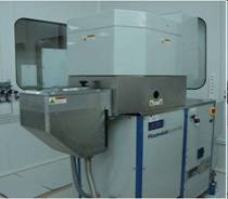
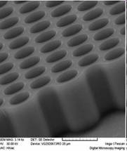
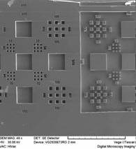
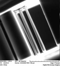
| DRIE- Plasmalab System 100-
ICP Deep Reactive Ion Etching System |
Contact persons: Andrei Avram, PhD stud; Marioara Avram, PhD
|
|
Applications:
- Etching:
- Bosch process for silicon
- Cryogenic process for silicon
- Bosch Process for SiC
- Single wafer processing.
- Can process 4” or smaller wafers, even small pieces.
- Process gases: SF6, C4F8, O2, Ar.
|
|
General characteristics:
- Single 4” wafer processing
- 5.000 W maximum ICP power
- 300 W maximum substrate electrode power
- Temperature control for substrate electrode
- 2 ultrafast MFC close coupled to the ICP source (for smooth sidewalls)
|
|
Process characteristics are:
- Si etch rate: 7.5 μm/min
- wafer non-uniformity: less than 3%
- wafer to wafer non-uniformity: less than 3%
- etching profile: 90o±1o vertical side-walls
- selectivity: 50:1 for PR mask or 200:1 for SiO2 mask
- aspect ratio: 20:1
|
|
 |
 |
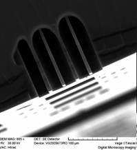 |
Advantages:
- High etch rate for etching deep trenches
- High ething uniformity
- High selectivity for photoresist and SiO2 masks
- Cryogenic process for perfectly smooth sidewalls
|
|
|
|
| |
| |
| |
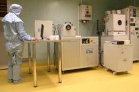
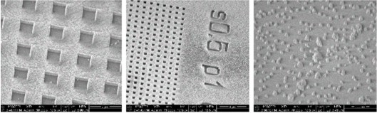
| Reactive Ion Etching (RIE) Plasma Etcher- Etchlab 200 |
Contact persons: Andrei Avram, PhD stud; Marioara Avram, PhD
|
Applications:
Typical applications for the basic configuration are:
- the etching of dielectrics (SiO2, Si3N4),
- semiconductors (Si),
- polymers and metals (Au, Pt, Ti, Ni).
General description:
The Etchlab 220 is a single wafer Reactive Ion Etching (RIE) machine. The substrates (wafer, carrier, small pieces) are directly loaded onto the substrate electrode after venting and opening the reactor. The control of the process can be manual or automated, using the included Sentech software. The recipe is controlled directly through the software, the gas concentration can be easily set by the technician. |
|
|
Characterization:
-
High etch rate
-
Low damage
-
Superior homogeneity
-
Remote field control via serial field bus
-
SENTECH’s plasma process systems operating software
-
Through-the-wall installation
-
Interferometric endpoint detection and etch depth measurement
|
|
|
| |
| |
| |
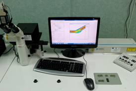
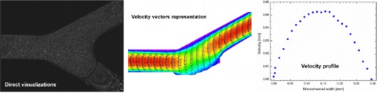
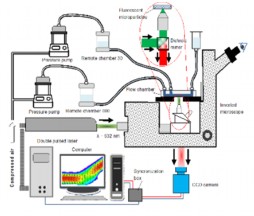
| Micro-PIV- PIV for Microfluidics (Particle Image Velocimetry) |
Contact persons: Catalin Mihai Balan, PhD; Catalin Marculescu PhD
|
Applications:
- Mapping concentration or temperature distributions in micro-flows.
- Measurements in microfluidic systems in chemistry, bio-chemistry, medical devices, DNA analysis, electronic cooling systems, micro-mechanical systems, micro total-analysis systems.
- Imaging-based measurements in microfluidic systems.
|
|
General description:
-
Particle Image Velocimetry (PIV) is a robust technique for measuring fluid velocity.
-
Workstation for microscopic imaging applications.
-
The method is an optical, non-intrusive technique measuring the movement of small tracer particles by means of a camera and pulsed laser light.
-
With this technique the flow velocity fields are mapped in 2D.
|
|
System architecture:
-
Microscope:
- Hi-Performance Leica Inverted Microscope.
-
Acquisition and control units
- 80N77 Timer Box
-
Camera
- Hi-Sense 4M cooled camera
-
Illumination
- Micro-Strobe. Green.
- Dual-Power 65-15 Laser 2x65 mJ at 15 Hz, 532 nm
|
 |
|
|
|
| |
| |
| |
| Wafer Bonder System- SB6L- Wafer - Substrate Bonder System |
Contact persons: Andrei Avram, PhD stud; Catalin Mihai Balan, PhD;
|
Applications:
General Characteristics :
-
Lower hot bond chuck with temperature control from ambient to 500oC
-
Negative High Voltage DC power supply for Anodic bonding
-
Flexible process: can accommodate polymer and adhesive bonding of different substrates
|
|
|
 |
Performance:
-
temperature control ± 3oC
-
temperature uniformity ± 2%
-
up to 8kN applied force
-
process vacuum pressure down to 5*10-4 mbar
Advantages:
-
Strong durable bonds
-
Excellent for encapsulation
-
Excellent for enclosure of fluidic microchannels
-
User friendly recipe editor for non-standard processes
|
|
|
| |
| |
| |
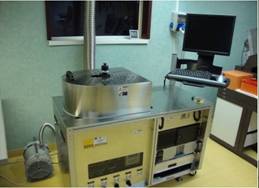
| Refractometer for layer thickness measurements - NanoCalc-XR |
Contact persons: Andrei Avram, PhD stud; Catalin Marculescu PhD
|
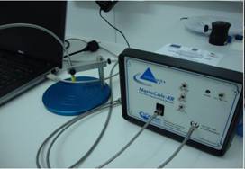 |
Applications:
-
Studies of various materials thickness on small scales.
-
Accurate measurements of grown or deposited thin films.
-
The provided information is useful for optimising silicon oxide growth or deposition of oxides and nitrides in LPCVD and PECVD equipments.
-
Provides useful information regarding spin coated polymers and photoresists.
-
Measurement of refractive index
|
|
General characteristics:
- Transmission and reflection measurements of anti-reflective & hardness coatings
- Wide wavelength measurements (250nm to 1050 nm)
- Can measure up to 10 layer stacks
- Angle of incidence: 90o
|
Performances:
- Resolution: 0.1 nm
- Thickness range: 10nm to 100μm
- Defect and roughness tolerant measurements
- Database for a broad range of materials
- Fast measurement process: 100ms to 1s
|
|
Advantages:
- Easy to use
- Wide measurements range
- Can measure thicknesses for a wide range of materials
- Small footprint: light and portable
- Assisted by powerful computational software
|
| |
| |