
NANO components for electronic SMART wireless systems
Type of the project: Prizes for participation in Horizon 2020 |
NANOSMART project has received funding from the European Union’s Horizon 2020 Research and Innovation Programme under Grant Agreement No. 825430 |

Results, stage 1
The scientific and technical report for Year 1 (in Romanian) cand be found here.
The project objectives provided for each activity have been fully achieved. The main results obtained in 2021 were the following:
Within IMT, antennas and patch antenna areas were simulated, manufactured and characterized with a graphene material called nanocrystalline graphite (NCG) with an operating frequency of 24 GHz.
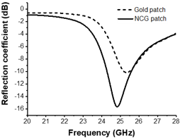
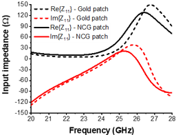
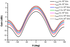
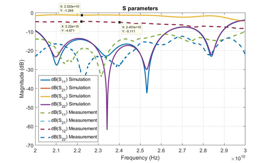
1) The antenna simulation was performed with a 3D electromagnetic simulator - CST Microwave Studio® using the optimal antenna parameters to obtain good results in terms of reflection loss and gain. Coplanar line technology (CPW) was used with an HRSi substrate covered with a thin dielectric layer of SiO2 and the antenna patch is made of a thin layer of NGC, the coplanar lines are made of gold and a thin layer was deposited on the back of the plate. aluminum as a reflective plane. The dimensions of the CPW line (50 impedance) are compatible with the CPW sample measurement system with a pitch of 150 μm. The simulation results show that the antenna has a very good reflection, a resonance in the 24-25 GHz band and a radiation efficiency of 31% with a gain of 0.3 dBi, a very good result since the single-layer graphene antennas have a low radiation efficiency. of only 2-3% and therefore a low gain with negative values. The results were obtained from the NCG conductivity measurement which was 16000 S / m. We find a variation of the gain between -1.62 dBi and 0.85 dBi, while the resonant frequency varies by 130 MHz. A linear array of the 8-element antennas was electromagnetically simulated, given that the gain increases in direct proportion to the number of antennas. The simulations were performed under the following conditions: the antenna area was designed in free space and on a 9 mm Plexiglas support under the HRSi substrate (used for measurements). The results of the simulations show that the array 8 elements NCG antennas has similar performances with an area with the same number of gold antennas, but the radiation efficiency is lower in the case of NCG.
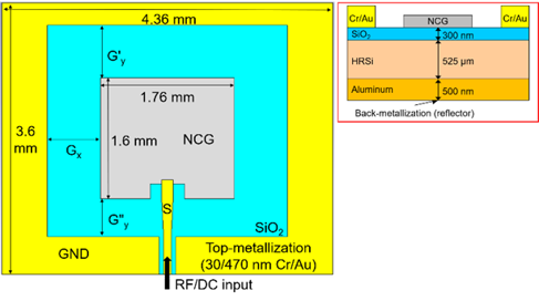 |
Top-view of the final NCG-CPA with the NCG layer as radiating element. Inset: cross-section of the antenna. |
 |
 |
|
a) |
b) |
|
|
||
c) |
||
. Simulated (a) reflection coefficient |S11| (dB), (b) input impedance Z11 () (black lines: real part; red lines: imaginary part), and (c) gain at 24 GHz (black lines: H-plane; red lines: E-plane; inset: visual explanation of H- and E-plane) of the single NCG-CPA and Au-CPA. |
||
|
||
|
||
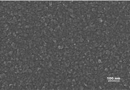
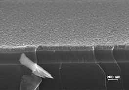
Patch antennas and 8-element antenna array were manufactured using coplanar line technology on HRSi/SiO2/NCG substrate. The NCG deposition process was performed in NANOFAB 1000 equipment (Oxford Instruments, UK), using a PECVD (plasma enhanced chemical vapor deposition) process on a Si/SiO2 (thermally enhanced silicon oxide with a thickness of 300 nm). The NCG thin film was corroded to make the patch antennas, the corrosion rate being about 50 nm/min, the total etching time being about 2 minutes. The complete removal of NCG from areas exposed to oxygen plasma was determined by 4-point electrical measurements. The metallic Cr/Au film (10/490 nm) deposited on the face of the wafer was configured using a lift-off process. Initially, the AZ1514 photoresistor was centrifuged and configured, followed by a metallic Cr/Au deposition. The photoresist was then removed using acetone in an ultrasonic bath. To protect the metal paths already configured during the technological processes performed on the back, after cleaning the platelet in acetone and IPA, photoresistor AZ1514 was centrifuged again on the front of the platelet. A metallic Cr/Au film (10/490 nm) was deposited on the back of the wafer, after which the photoresist AZ1514 was centrifuged and configured. The metal film was corroded in specific solution, after which the plate let was cleaned in acetone and IPA.
 |
 |
||||
a) |
b) |
||||
EM images for (a) top-view and (b) cross-section of the fabricated NCG thin film |
|||||
|
|||||
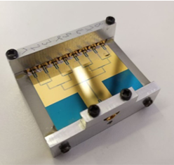
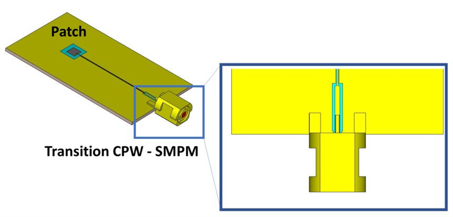
Mounting the antenna on Plexiglas support and connecting it with the SMPM connector. |
|||||
 |
|||||
|
|||||
|
|||||
|
|||||
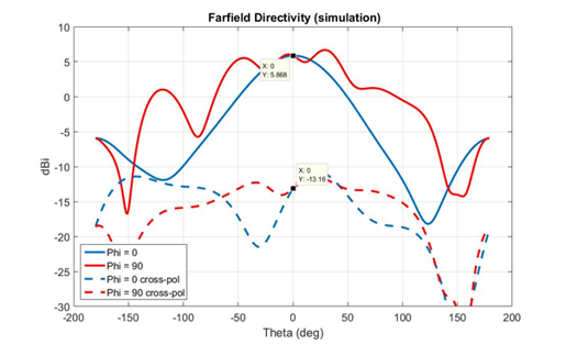
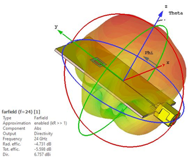
3D simulated diagram radiation for NCG. |
|||||
 |
 |
||||
Antenna array weith 8 elements based on NCG |
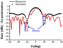
Measured (solid red curves) and simulated (dotted black curves) gain in the H-plane for both co-polarization unbiased NCG based antenna array |
||||
Activitatea de diseminare a cuprins 1 lucrare publicata in revista ISI„ IEEE Access:
M. Aldrigo, M. Dragoman, S. Iordanescu, A. Avram, O.-G. Simionescu, C. Parvulescu, H. El Ghannudi, S. Montori, L. Nicchi, S. Xavier, and A. Ziaei, Tunable 24-GHz antenna arrays based on nanocrystalline graphite, IEEE Access 9, pp. 122443 – 122456 (2021).
Estimated results
The expected quantifiable result is the fabrication of a nanocrystalline graphene (NCG) based patch antenna which will be obtained as follows:
- the nanocrystalline graphene (NCG) film with a thickness of about 100 nm will be grown on High-Resistivity Silicon / Silicon Oxide (SiO2);
- the NCG based patch antenna, with operating frequency in the ISM 24 GHz band, will be manufactured in coplanar waveguide (CPW) technology for on-wafer measurements using standard measuring probe tips. The metal contacts will be made of gold, with a thickness of about 500 nm.
The expected quantifiable impact is an antenna with a reconfigurable resonance frequency up to 150 MHz (typical) and a reconfigurable gain of up to 3 dB (typical), which represents a halving / doubling of the transmitted (received) power .