
Results
Results obtained in 2024
In this last stage, is evidenced the interaction between the magnetic field and surface acoustic waves through a ferromagnetic material, in the SAW type device and the behavior of SAW structures at cyogenic temperatures as magnetic sensors.
In this stage, the following objectives were achieved:
- Simulation of the magnetic behavior of SAW devices on ScAlN/Si at cryogenic temperatures;
- Fabrication of SAW structures on ScAlN/Si for the SAW/SW coupling and for the magnetic sensor;
- Characterization of SAW structures on ScAlN/Si (Rayleigh and Sezawa modes) in magnetic field at room temperature and at cryogenic temperatures;
- Magnetic field characterization of sensor structures manufactured on ScAlN/Si.
1. Simulation of the behavior of SAW devices on ScAlN in magnetic field at cryogenic temperatures, as magnetic sensors
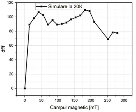
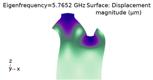
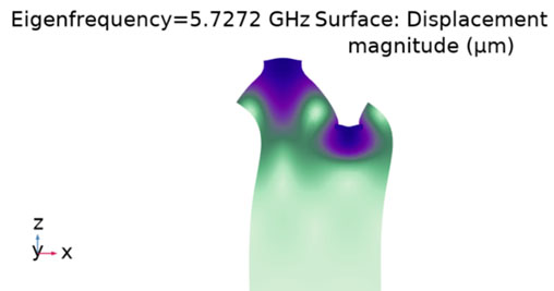
The behavior of SAW devices fabricated on ScAlN at cryogenic temperatures as a magnetic sensor was simulated. The materials used for simulation are Ni for the metallization, Sc0.3AlN0.7 as piezoelectric material and the substrate of Si. From a geometry point of view, the metallization thickness is 50 nm, the piezoelectric material has a thickness of 0.8 μm and the Si thickness was chosen to be 15∙λ. The width of the electrode in the IDT component was chosen to be 170 nm. The simulation was performed by modifying the Young's modulus of elasticity and the fitting of the results with those at room temperature. From the simulation at room temperature, the Rayleigh resonance frequency was determined at 5.7272 GHz. At a temperature of 20 K from the simulation, the resonance frequency of 5.7652 GHz was obtained. From the identified values of the Young's mode, the corresponding values were chosen for the simulation at 20 K. Thus, it was possible to determine the variation of Δf/f as a function of the applied magnetic field, at a temperature of 20 K, with a higher value than that for room temperature.
Rayleigh mode at room temperature |
 |
 |
|
Rayleigh mode at 20K |
df/f variation function of magnetic field at 20K |
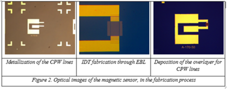
2. Fabrication of SAW structures on ScAlN for magnetic sensor and SAW/SW coupling and non-reciprocity
Three runs were planned for fabrication in the last stage of the project, the designed structures being used either as magnetic sensors (with wavelengths of 400 nm and 680 nm) or for SAW/spin wave (SW) coupling. The technology was similar to that used in the previous phases, the steps followed being the following: CPW line from Ti/Au, with a thickness of 100 nm (10 nm Ti, 90 nm Au) through a lift-off process; the interdigital area through EBL, with Ti/Au metallization, with a thickness of 50 nm (5 nm Ti, 45 nm Au), also using a lift-off process; thickening of the CPW line by depositing a 250 nm thick Ti/Au layer (20 nm Ti, 230 nm Au), through a lift-off process; deposition and configuration of the 12 nm thick ferromagnetic Ni layer, over which a thin Pt layer (3 nm) was deposited. For the runs manufactured in this stage, high resistivity Si wafers (>10000 Ωcm) with a ScAlN layer thickness of 830 nm were used.
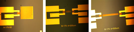 |
Imagini optice ale structurilor SAW pe ScAlN |
3. Characterization of SAW structures on ScAlN/Si (Rayleigh propagation modes) in magnetic field; the influence of heavy metal on the non-reciprocity of SAW structures on ScAlN/Si
S parameters were measured with/without an applied magnetic field μ0H, to evaluate the coupling (absorption and non-reciprocity) SAW-SW, characteristic of structures with a ferromagnetic layer (FM) between the IDTs, when we have/don't have a heavy metal deposited on the FM.
Three SAW structures on ScAlN/Si with two ports and a Ni/Pt layer (12/3 nm) (between the two IDTs) with wIDT=170nm were characterized, which were compared to the same type of structure, which was characterized in the previous stage, but having a Ni/Au magnetostrictive layer. The goal was to observe the variation of the non-reciprocity ΔS and μ0δHa_res in magnitude, respectively in the resonance magnetic field, with the chosen heavy metal.
The Ni/Pt layered SAW structures were analyzed only for the Rayleigh mode, because the Sezawa acoustic transmission value, |S21TG|<-76dB, was not acceptable. Comparing the structures with Ni/Pt layer with the structure with the Ni/Au layer, it can be seen that the absorption at θ=45° was slightly better for the structures with Ni/Pt than for the structure with Ni/Au; likewise, the non-reciprocity was slightly higher for the structures with Ni/Pt than for the structure with Ni/Au.
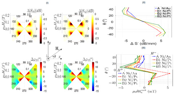 |
Asymmetric polar plots of absorption Δ|Sij|(up) and phase change Δ|ϕij|( down) as a function of the magnetic field μ0Ha and the angle θ for Ni/Pt sample at the resonance frequency SAW fres=5.1 GHz. Zoom on values of μ0Ha∈[0, 0.2] T. Non-reciprocity in magnitude ΔS− (II) and in magnetic field μ0δHa res± (III) as a function of the angle θ for the four samples studied. |
In this stage, is evidenced the interaction between the magnetic field and surface acoustic waves through a ferromagnetic material, in the SAW type device.
Following objectives were achieved:
- Simulation of the magnetic behavior of SAW devices on ScAlN/Si;
- Fabrication of SAW structures on ScAlN/Si for the SAW/SW coupling and for the magnetic sensor;
- Characterization of SAW structures on ScAlN/Si (Rayleigh and Sezawa modes) in magnetic field at room temperature and at cryogenic temperatures;
- Magnetic field characterization of sensor structures manufactured on ScAlN/Si.
1. Magnetostrictive simulation of SAW device on ScAlN/Si at room temperature
The strain and stress values that appear in the Ni layer when the magnetic field is applied were determined. The average stress on each face of the nickel metallization (ferromagnetic domain) was calculated for each element. Figure 1 shows the magnetic field distributions (a), the displacement distributions (b) and the von Mises stress distributions (c), at the value of 7 mT and the displacement distribution for B = 294 mT (d).
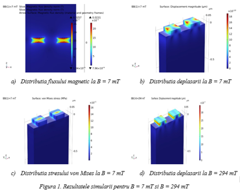 |
On each side of the ferromagnetic field, the average value of the stress tensor was calculated for each direction.
2. Fabrication of SAW structures for magnetic sensor
 |
3. Characterization of SAW structures on ScAlN/Si in magnetic field (Rayleigh and Sezawa propagation modes)
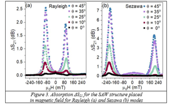
The S parameters were measured and were observed two propagation modes: the Rayleigh propagation mode, at the resonance frequency of 4.67 GHz and the Sezawa propagation mode, at the frequency of 8.04 GHz.
The coupling of the spin waves with the SAW acoustic wave is evidenced by the decrease in the amplitude of the transmission parameters (S21, S12) (dB), called absorption, due to the transfer of energy from the SAW wave to the spin waves. This coupling is maximum when the angle between the applied magnetic field and the propagation direction of the SAW wave is 45°. Figure 3 shows that the maximum absorption in the magnetic field occurs at -90mT for Rayleigh mode and has a value of 2.54dB. For the Sezawa mode, the maximum absorption occurs at a magnetic field of -203mT and has a value of 7.24dB.
 |
________________
Estimated results
- Manufacturing and characterization of SAW structures on ScAlN/Si with finger and finger/interdigit spacing width between 80-170 nm and magnetostrictive material, Ni and/or CoFeB of different thicknesses (in the range 10-45 nm) between the IDTs with resonance frequencies above 4 GHz;
- Analysis of SAW/SW coupling at different angles between magnetic field strength and the SAW propagation direction, performed at room and cryogenic temperatures, for Rayleigh and Sezawa propagation mode. A higher coupling than that reported for other types of materials is expected.
- Nonreciprocal behavior analysis at room and cryogenic temperatures, for SAW structures manufactured on ScAlN/Si, for Rayleigh and Sezawa propagation mode
- Simulation of ScAlN SAW based structures for magnetic sensing at room temperatures and cryogenic temperatures
- Characterization as magnetic sensor at room temperature and also at cryogenic temperatures of single port SAW structures with Ni deposited in the IDTs composition as well as magnetic layers (Ni si/sau CoFeB) in the vicinity of the active IDTs area
- Submission minimum 3 papers in high ranked journals (Q1 or Q2); Minimum 5 participations at conferences two of them where the acceptance rate is <50%; 1 patent.