
Results
Results, December 2024 (in Romanian)
Attempting to enhance the solar cell efficiency, the photovoltaic (PV) research community seeks also the reduction of the fabrication costs of solar cells by using a low cost, large diameter substrate from a material which is abundantly available on earth, such as silicon. Thus, a true monolithic integration of the III-V semiconductors structures with silicon is receiving great interest since it will enable simultaneous high efficiency and low cost manufacturing. The group III-nitride alloys, such as InGaN, has the unique advantage of one of the widest adjustment of direct bandgaps from 0.65 eV (InN) to 3.42 eV (GaN) range. Compared to Si, GaAs, CuInGaSe, or Ge systems, it is the only semiconductor system that provides the perfect match to the solar spectrum (0.5 to 4 eV), which opens up an interesting opportunity for high-efficiency tandem cells. Thus, lots of efforts have been devoted so far into using InGaN as an absorber in Si-based solar cells. However, despite challenging results, the use of InGaN as a veritable PV material is still at early stages mainly due to the severe deterioration of material quality with In incorporation at high concentrations necessary to acquire the desired low bandgap in a tandem cell. The project has proposed to alleviate this annoying bottleneck in development of InGaN/AlN/Si solar cells by proposing an innovative BGaN material capable to be lattice compatible to AlN, yet allowing the desired bandgap shrink.
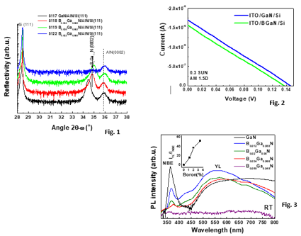
Thus, using an advanced growth technique, namely, molecular beam epitaxy (MBE), ternary compunds BGaN/AlN/Si(111) have been grown by MBE, as seen in Fig (1). Incorporating next the sintesized material in a solar cell structure on Si(111) has been seen to be accompanied by an undesired drop in shortcircuit current and opencircuit voltage comparing to a reference GaN-on-Si(111), as depicted in Fig. 2. While reduction of the photovoltage could be associated to the decrease in the bandgap of the BGaN compared to GaN, the decrease in the generated photocurrent suggests that despite strain compensation with respect to AlN/Si the presence of B leads unavoidable deterioration of the host semiconductor matrix. Indeed, such B-induced deterioration has been found to start even at low boron concentrations, as demonstrated experimentally (see Fig. 3).
 |
Results, December 2023
Hexagonal boron nitride (h-BN), a two-dimensional (2D) wide-band-gap semiconductor material (Eg ≈ 5.96 eV), is attracting high interest for its excellent properties and wide range of possible applications, owing to high band-edge absorption coefficient, low dielectric constant, superior breakdown field, high thermal conductivity, and good thermal, mechanical and chemical stability. The growth of wafer-scale high-quality h-BN monolayer or few monolayers on appropriate substrates is the prerequisite for their various potential applications. Recently, the scalable growth of mono and few-layer h-BN has been achieved on catalyzing metal substrates. However, the use of metal substrates usually needs an additional transfer process from metal substrates to semiconducting or insulating substrates for most device applications. The complicated transfer process is not only cost-intensive but also introduces contamination and mechanical damage. Therefore, the direct growth of few-layer h-BN with high structural quality on microelectronic compatible dielectric substrates is highly desirable. Because of the low catalytic activity of dielectric materials, such as sapphire, it is difficult to directly nucleate h-BN on sapphire substrates, leading to a poor crystallinity of h-BN layers. To compensate for the poor catalytic activity of dielectric substrates, extremely high substrate temperatures (1350−1700 °C) are usually required to achieve the direct growth of h-BN. However, such high substrate temperatures are notonly unavailable for most equipments but also not compatible with most commonly used substrates or integration with organic compounds, where temperatures close to room temperature (RT) are required to prevent the organics degradation.
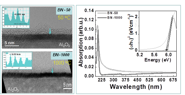 |
In a collaborative work involving research groups from Romania, Spain and Germany it has been recently shown that high-quality ultrathin sp2-BN material can be grown on sapphire substrates not only at the high temperature of 1000 oC (BN-1000) but also at the much lower temperature of 50 oC (BN-50) by molecular beam epitaxy. By our knowledge, This is, so far, the lowest temperature ever used for the synthesis of sp2-BN materials by a growth technique. The next step is to develop BN/AlN_on_Si templates by growing thin layers of sp2-BN on top of AlN_on_Si substrates.
______________
Estimated results:
1) The incorporation by MBE of at least 8% B into GaN while maintaining the lattice matching condition to the low-costs AlN-on-Si structures.
2) The growth and processing of a lattice-matched BGaN/AlN-on-Si solar cell.
3) Al least 5 ISI papers cu high impact factor and 3 presentations at international conferences.
4) One request for invention brevet.