PHOTONTECH
|
| Home | |
| Partners | |
| Objectives | |
| Resources | |
| Activities/Results | |
| Publications | |
| Related EU Projects | |
| Events | |
| Contact |
Activities (1)
Silicon micromachining for microphotonics
SOI –based microphotonic components (micro-mirrors, optical waveguides)
Process steps:
- Si etching (RIE)
- SiO2 etching in HF solution
a)
b)
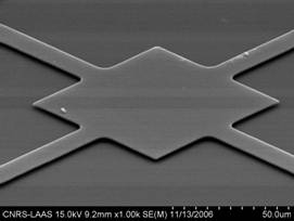
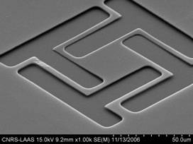
c)SEM images of suspended SOI-based microstructures: a) movable micromirror 100x100 mm2 b) movable micromirror 50x50 mm2; c) bridge.
Si thickness: 2 mm; air gap: 2 mm
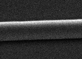
a)
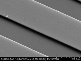
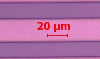
b)silicon optical waveguides on SOI wafers: aoptical magine; b) SEM imagine
Si thickness: 2 mm; SiO2 thickness 2 mm