Project Results
Stage 1/2017. Design, fabrication and characterization of SAW resonator test structures, tuned with printed lumped elements processed on GaN/Si
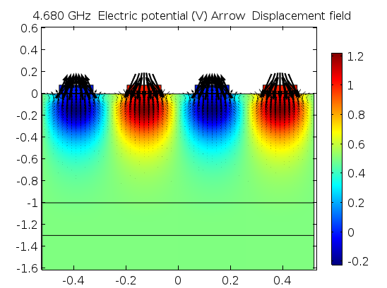
During this stage, numerical models for the multiphysical simulation of the SAW resonators were developed using COMSOL Multiphysics software. Based on these models, the electromechanic field distributions (electric potential and displacement) for different propagation modes (Fig. 1) were investigated for the case of a 1 µm thick GaN layer, grown through MOCVD on a high resistivity silicon substrate. The cases of gold and aluminium metallization were presented.
3D electromagnetic models were developed using CST Studio Suite (Fig. 2) for the simulation of the SAW resonators and the printed lumped elements. The models are based on the local modulation of the substrate permittivity using the Lorentz dispersion model. Different structures were simulated, and the effect of the length of an inductive line, as well as of the area of the SAW resonator was shown.
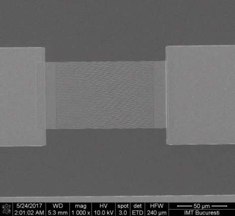
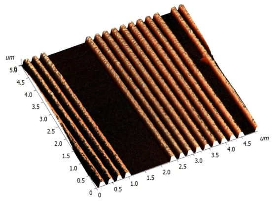
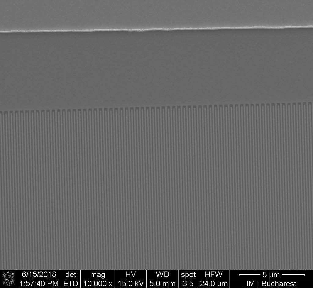
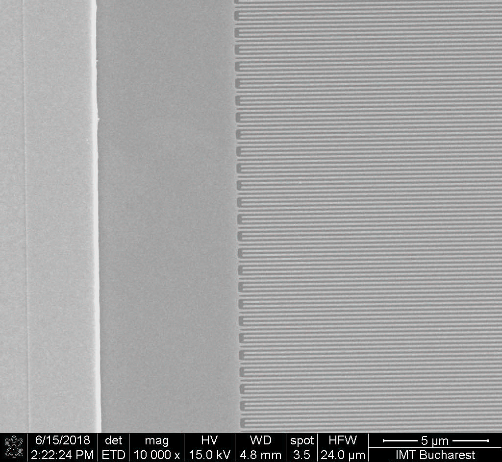
Test structures and their corresponding processing mask sets were designed for Run 1. Run2 included the building blocks for the band pass filters. The structures were fabricated using a 3-step technological process, optimized for the thin metal layer requirement of the SAW resonator and the thick metal layer requirement of the contact pads, CPW transmission lines, lumped element printed inductors. The structures were characterized structurally using SEM (Fig. 3 and Fig. 4) and AFM (Fig. 5) investigations and the quality of the technological process was demonstrated.
The microwave characterization was performed by means of S-parameter pn wafer measurements (Fig. 6). The results demonstrated the coverage of the whole frequency range of interest for the proposed band pass filters. The equivalent circuit based modelling involved defining new model parameters besides the static capacitance: the quality factor, series resonance and the effective coupling coefficient.
The model parameters were extracted from experimental data and, based on the results obtained for a large number of measured structures, their dependence as a function of the SAW resonator area was plotted. The mean value of 800 obtained for the quality factor and the values of about 0.08% of the coupling coefficient will ensure the performance of the band pass filters which will be designed in Stage 2.
 |
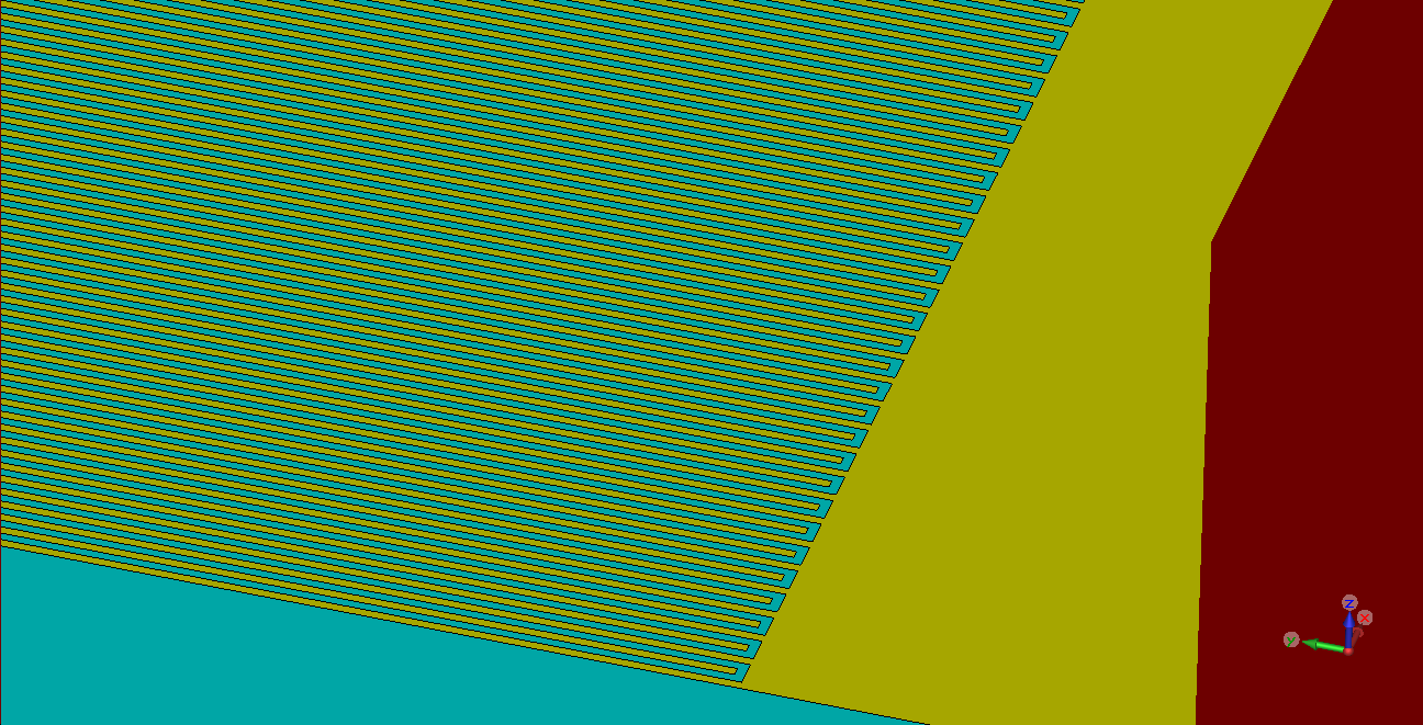 |
Fig. 1. 2D COMSOL model |
Fig. 2. 3D EM CST Model |
 |
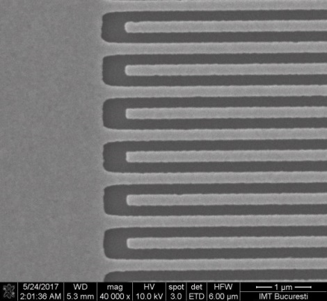 |
Fig. 3. SEM image of fabricated SAW |
Fig. 4. SEM image: detail of 200 nm wide digits |
 |
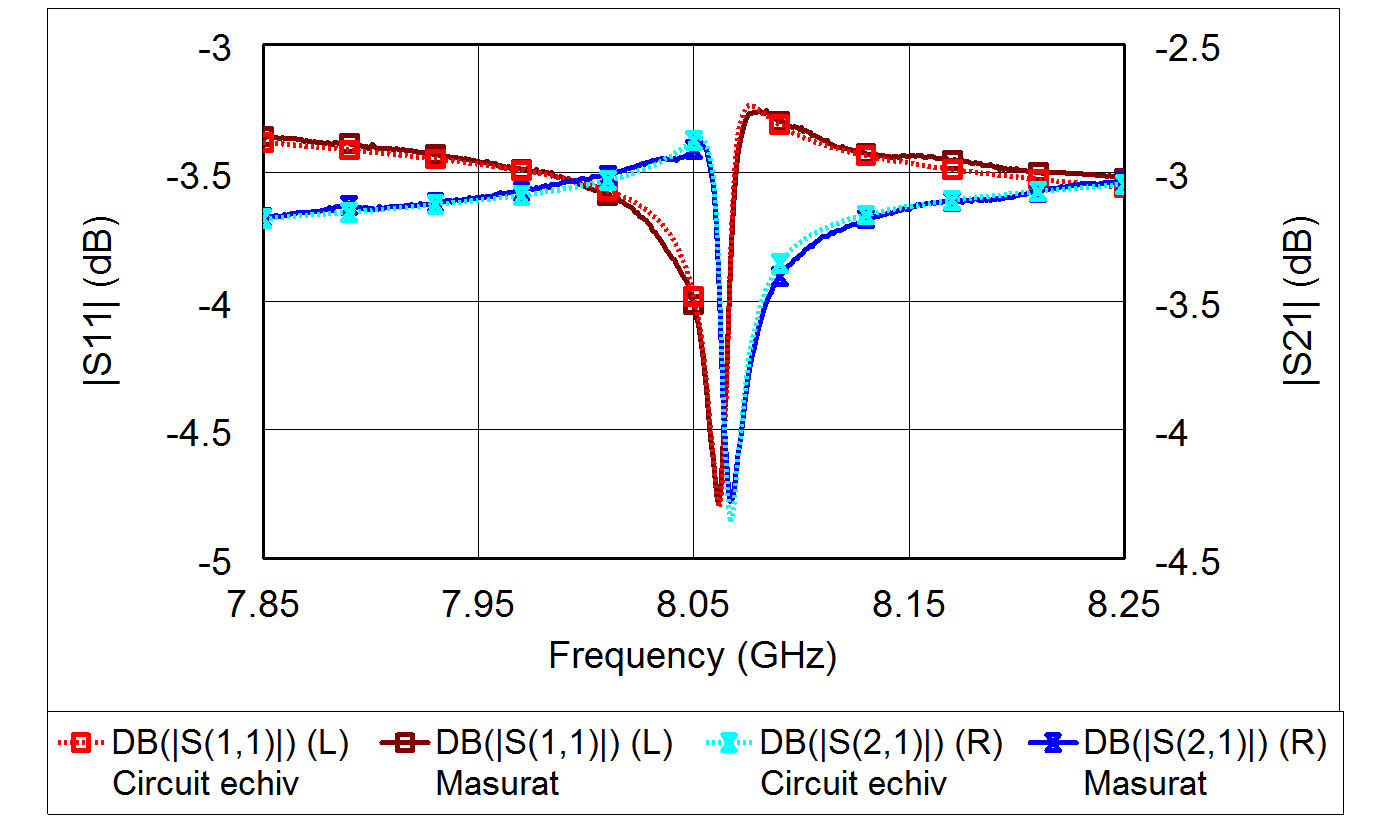 |
Fig. 5. AFM image: 130 nm wide digits |
Fig. 6. Comparison of measured/equivalent circuit S parameters for a SAW with 130 nm wide digits |
Stage 2/2018. SAW band pass filter demonstrators tuned in frequency using printed lumped elements
In the frame of this stage the specifications for the band pass filter were established (central operating frequencies, insertion losses in the pass-band, out of band rejection, bandwidth). Based on the performances of surface acoustic wave structures processed on GaN/Si found in literature, as well as on the experimental results obtained in Stage 1/2017, and simulated results determined in the current stage, the final specifications for the demonstrators operating in the following frequency ranges were determined: 3.7 – 4.2 GHz, 5.9 – 6.4 GHz, 7 – 8.5 GHz. In addition to these frequency ranges, specifications were added for filters operating at frequencies above 9 GHz.
Five demonstrator structures were designed and optimized, based on interdigital transducers (IDT) with electrode widths between 150...100 nm, with three configurations. The first type (normal - Fig. 7) consists of a simple structure with digits connected alternatively to the two electrodes. The second configuration is called DART (Distributed Acoustic Reflection Transducer - Fig. 8) and is constructed by connecting three digits to one electrode and the fourth digit to the other electrode. This 4 digit period is then repeated. The third configuration is called Split (Fig. 9) and is obtained by connecting two digits to each electrode. The Split and DART IDTs were monolithically integrated with meander inductors and optimized for reflection losses below -10 dB (demonstrators 1A and 1B) (Fig. 11). The normal type IDTs with electrode widths of 150 nm were integrated with strip type inductors (demonstrator 2). The IDTs with electrode widths of 130 nm and 100 nm were monolithically integrated with strip inductors in a PI-type filter configuration (demonstrators 3 and 4, respectively). The final layout was obtained through co-simulation using electromagnetic and circuit level optimization.
In order to successfully obtain 100 nm wide digits/interdigits, a metallization of 5/45nm Ti/Au was used. In this case the technological process consisted of 3 main steps: 1. Deposition and lift-off of the nano-lithigraphic alignment marks and CPW circuit alignment marks; 2. Electron beam lithography of the interdigitated structures and deposition and lift-off of the 4/45 Ti/Au metallization; 3. Deposition and lift-off of the CPW circuits (5/300 nm Ti/Au). For steps 1 and 3 dedicated glass and Chromium masks were fabricated (Fig. 10). The normal type structures with digit/interdigit of 130 nm and 150 nm were fabricated with a metallization of 5-95 nm Ti/Au and 70 nm Al, respectively, using the technological process developed in Stage 1/2017.
The filter structures were characterized on wafer using a Vector Network Analyzer. The most significant results were obtained for the 8 GHz filter (with 130 nm electrodes). For a structure of only 0.75 x 2.9 mm2, insertion losses of 13.2 dB and an out of band rejection of almost 30 dB were obtained. The – 3dB bandwidth is 20 MHz. These results are beyond the state of the art for surface acoustic wave based filters processed on GaN/Si and open the way towards new X-band (8 - 12 GHz) communications applications.
 |
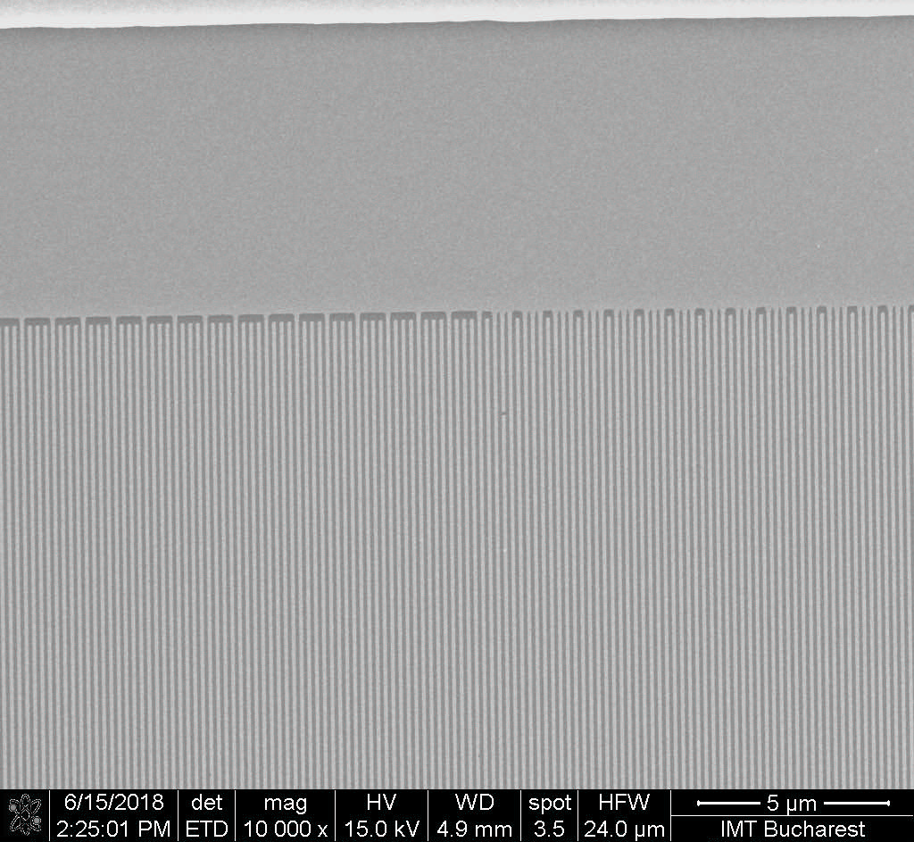 |
Fig. 7. Normal IDT with 100 nm electrodes |
Fig. 8. DART IDT with 100 nm electrodes |
 |
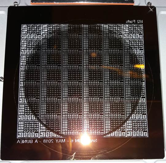 |
Fig. 9. Split IDT with 100 nm electrodes |
Fig. 10. Photo of a processing mask |
 |
|
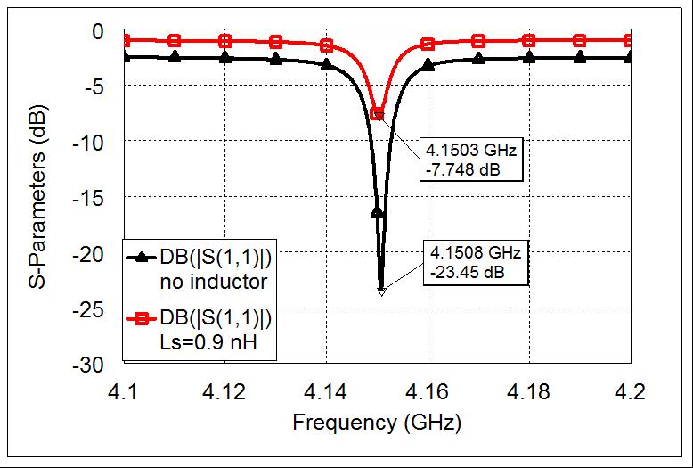
| Fig. 11. Effect of changing the value of the meander inductor by adding a series inductance of 0.9 nH | |