
Welcome to MoMiCom website!
Monolithic Millimeter wave Front-End for Advanced Communications
Results
| Dissemination | Results 2022 |
| Results 2021 | Results 2020 |
The 3rd stage of the project focused on the integrated millimeter wave front-end and was divided into the following tasks: Task 3.1. System integration; Task 3.2. Integrated front-end fabrication; Task 3.3. Characterization of the integrated front-end. The main results obtained during the reporting period are: the layout files for the PCB and 3D dielectric lens; the GaAs millimeter wave integrated front-end; tangential signal sensitivity measurements for the integrated front-end. One ISI conference paper and one ISI journal paper were published (with acknowledgement to the project). Another journal paper is currently being evaluated for publication in a Q2 ISI journal.
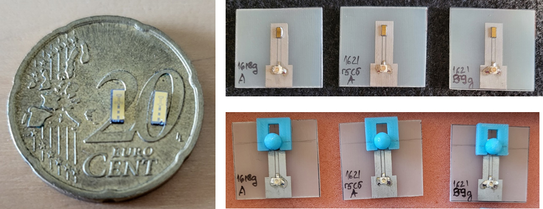
The receivers that are based on a Schottky diode detection circuit and monolithically integrated with a planar antenna were diced into individual chips and integrated with a dielectric lens fabricated through 3D printing. Support PCBs were designed and fabricated for the receiver chips.
 |
|
| Diced millimeterwave GaAs receivers | Receivers integrated on support PCBs with 3D printed lenses |
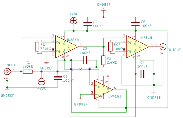
A low frequency video amplifier circuit for the extraction of the Schottky diode demodulated signal was designed and fabricated using SMD components. The circuit is based on the precision instrumentation amplifier INA818 from Texas Instruments (35-μV offset, 8-nV/√Hz noise) and uses the operational amplifier OPA191 in order to eliminate the DC offset generated by the DC bias of the receiver. The video amplifier was tested using a function generator at the input and a digital oscilloscope at the output. A voltage gain of 576 was measured, with a 3dB bandwidth >100 kHz and a lower frequency limit of 0.5 Hz. The circuit includes a DC bias network for the Schottky diode.
 |
 |
| Circuit schematic of the video amplifier | Receivers integrated on support PCBs with 3D printed lenses |
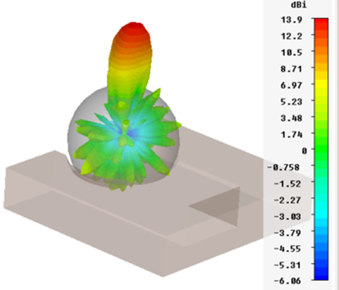
The dielectric lens was designed using full-wave 3D electromagnetic simulations. A compromise between size and directivity led to a 3 mm radius hemisphere with a 1.5 mm extension. The lens increased the directivity of the folded slot antenna by about 6 dBi. The structure was 3D printed using a generic polylactic acid (PLA) filament and fused deposition modeling (FDM) with 100 micron layer resolution and 100% infill. A support was added to ensure a distance of 2.75 mm to the antenna surface.
 |
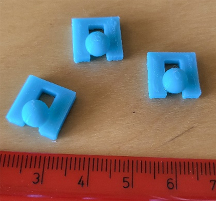 |
| Simulated 3D directivity characteristic at 90 GHz for slot antenna with dielectric lens | 3D printed dielectric lenses using PLA filament |
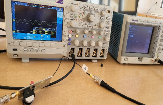
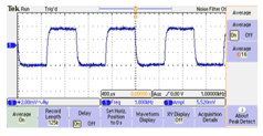
The sensitivity of selected receivers was measured in the 90 – 100 GHz range. The measurement setup consists of a W-band standard gain horn antenna fed with an amplitude modulated signal (1 kHz modulation frequency). The signal propagates through free space and is then picked up by the antenna of the receiver and demodulated by the Schottky diode. The resulting 1 kHz modulated signal is the input signal of the video amplifier and its output can be viewed on a digital oscilloscope.
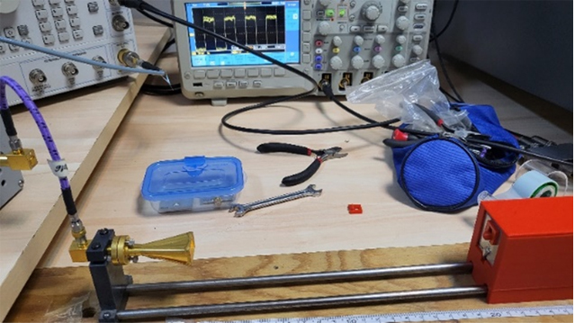 |
Measurement setup for receiver sensitivity assessment |
The isotropic voltage sensitivity is calculated as the ratio between the output voltage amplitude and the incident power. The measured results for the receivers developed in the frame of the project showed peak voltage sensitivities in the range of 12000 mV/mW in the 90 – 95 GHz frequency range. The detector noise equivalent power (NEP) was calculated at 12 pW/√Hz.
Conclusion and estimated project impact
The project successfully demonstrated a compact solution for GaAs based receivers for millimeter wave applications. A receiver monolithically integrating an antenna with a detection circuit and a filtering circuit has a total area of only 1.4 x 3.5 mm2 and a chip thickness of 0.4 mm. The reduced size recommends it for direct integration in mobile devices or hotspot type equipment for 5G communications in the above 80 GHz band. The receiver was validated through performance parameter measurements, such as the noise equivalent power and the isotropic voltage sensitivity, reaching an estimated technology readiness level (TRL) of 3. The results include the antenna performance and are comparable to current state-of-the-art W-band detector diodes.
Dissemination
IEEE Conferences (ISI indexed)
Alina-Cristina Bunea, Dan Neculoiu, Adrian Dinescu, “Characterization of 3-port SAW diplexers using 2-port VNA measurements”, International Semiconductor Conference, CAS 2022, Poiana Brasov, Romania, oct. 2022 (accepted for presentation)
ISI Journal papers
D. Neculoiu, A.C. Bunea, O.G. Profirescu, „Compact Implementation of an RFID Tag with Electromagnetic Wave Polarization Diversity”, Romanian Journal of Information Science and Technology, vol. 25, No. 2, 2022, pp. 170-178, WOS:000823109400005
A.C. Bunea, D. Neculoiu, A. Stavrinidis, G. Stavrinidis, A. Kostopoulos, G. Konstantinidis, „Monolithic integrated Schottky diode multiplier and rectenna for wireless communication link in the W band”, (under evaluation)
_____________
The 2nd Stage of the MoMiCom project corresponds to the following Tasks: 2.1. Fabrication of the receiving front-end building blocks (Run1); 2.2. Measurement of the receiving front-end building blocks (Run1) and parameter extraction; 2.3. Modeling and design of the receiving front-end demonstrator; 2.4. Fabrication of the receiving front-end demonstrator; 2.5. On-wafer measurement of the receiving front-end demonstrator (Run2). The following results were obtained during the reporting period: test circuits for the receiving front-end building blocks; on wafer characterization results for the receiver building blocks; mask set for the receiving front-end; fabricated receiver structures; on-wafer characterization results of the receiver structures. Two papers with acknowledgement to the project were published, one at a IEEE conference (ISI indexed) and one in a Q2 ISI journal.
The receiver building blocks designed in the previous stage of the project were fabricated on GaAs wafers with 5 different combinations of epi-layer thicknesses and doping levels. The passive elements, namely the low pass filter and antenna, were characterized on wafer by means of scattering (S) parameter measurements. The measured performances recommend the use of the passive building blocks in the design of the monolithic integrated receiver.
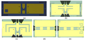 |
Fabricated receiver building blocks: (a) Schottky diode in CPW configuration; (b) detection circuit and matching network v1; (c) detection circuit and matching network v2; (d) low pass filter for signal extraction; (e) detection circuit with low pass filter.
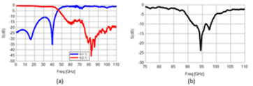 |
On wafer characterization results: (a) low pass filter; (b) antenna input matching
The diodes were characterized in direct current (DC) and radio frequency (RF) and the main parameters were extracted, namely the ideality coefficient, the saturation current, the series resistance, the junction capacitance and the cutoff frequency. Two epi-layer configurations, where the extracted cutoff frequencies of the diodes were over 1 THz were chosen for the fabrication of the monolithic integrated receivers.
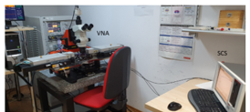 |
Measurement setup for on wafer characterization of the millimeter wave diodes: left – VNA with on wafer probing station up to 110 GHz; right – semiconductor characterization system (SCS-4200) for DC curve tracing and biasing.
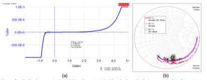 |
On-wafer diode characterization: (a) i-v characteristic (the diode cathode is connected at the output so negative voltage is required for forward region); (b) comparison of simulated and measured RF characteristic for a bias current of 100 µA |
The monolithic integrated receivers were designed by including the diode small signal model in the full-wave 3D electromagnetic model of the full receiver structure, which includes the antenna, the detector circuit (diode and matching networks) and the lop pass filter. The models were optimized for radiation reception in the W band (75 – 110 GHz). The resulting layout was then transferred to a mask design software and included in the fabrication mask set which consists of 6 photolithographic masks and one mask for electron beam lithography. The final size of the full receiver structure is 3.5 x 1.75 mm2, which corresponds to the project objectives.
A dedicated measurement setup was developed for the characterization of the receivers. The setup was based on emitting a W band signal, with an amplitude modulation of a few kHz. The demodulated signal was then recorded at the output of the test receivers and the frequency characteristics and 2D radiation characteristics (in H and E plane) for two different frequencies were plotted. Two receiver structures, which correspond to the two epi-layer configurations, were characterized on wafer using this procedure.
All objectives of the 2nd Stage of the project were successfully accomplished.
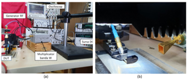 |
Receiver on wafer characterization: (a) measurement setup for the |
 |
Detected signal at the low pass filter output. |
DISSEMINATION
IEEE Conferences (ISI indexed)
-
D. Neculoiu and A. -C. Bunea, “RFID tag with electromagnetic wave polarization diversity”, 2021 International Semiconductor Conference (CAS), 2021, pp. 1-4, doi: 10.1109/CAS52836.2021.9604122. (Best Paper Award)
 |
ISI Journal papers
-
Bunea, A.-C.; Dediu, V.; Laszlo, E.A.; Pistriţu, F.; Carp, M.; Iliescu, F.S.; Ionescu, O.N.; Iliescu, C., „E-Skin: The Dawn of a New Era of On-Body Monitoring Systems”, Micromachines 2021, 12, 1091. https://doi.org/10.3390/mi12091091; WOS: 000701080700001.
The 1st Stage of the project corresponds to Task 1.1. Modeling and design of the front-end building blocks. 3D electromagnetic models were developed for planar antennas to be processed on GaAs substrate. The model parameters were defined as variables and the effect of the variation of different parameters on the radiation and input matching were assessed. Parametric studies were performed for operation optimization in the millimeter wave band, more exactly in the W band (75 – 110 GHz). The matching networks, low pass filter and DC bias path were designed using AWR Microwave Office, where the Schottky diode was included using its small signal equivalent model. A 3D model of the Schottky diode was developed using COMSOL Multiphysics software package. The mask files for the receiver building blocks (i.e. antenna, detector, low pass filter) were also designed.
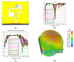 |
Simulation of antenna element: (a) 3D electromagnetic model of a 1.5 x 1.4 mm2 on chip antenna; (b) parametric simulations of the effect of the d_cut parameter on the input matching; (c) parametric simulations of the effect of the d_cut parameter on the directivity in the direction normal to the antenna plane as a function of frequency; (d) optimizaed 3D radiation pattern.
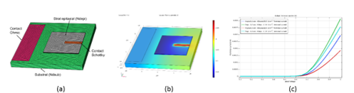 |
COMSOL Multiphysics modeling: (a) 3D model of the Schottky diode and volume discretization; (b) free charge distribution for 1 V; (c) i-v characteristics as a function of the epi-layer doping concentration
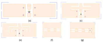 |
Mask files for the receiver building blocks: (a) Schottky diode in CPW configuration; (b) detection circuit with v1 matching network; (c) detection circuit with v2 matching network; (d) low pass filter for signal extraction; (e) detection circuit with low pass filter
All objectives of the 1st Stage were successfully accomplished.