| |
Structuring technologies at the nano scale based on Electron Beam Lithography and related techniques |
| |
| |
- developing and refining nano-structuring technologies based on Electron Beam Lithography patterning; |
| |
- design and fabrication of nanostructures by EBID and EBIE; |
| |
EBID technique has been used in order to obtain Pt, W and SiO2 nanostructures |
| |
|
|
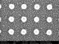
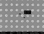
SiO2 nanodots (70 nm diameter)
deposited by EBID on Si |
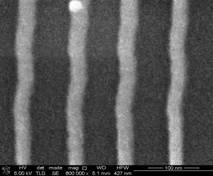
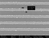
Tungsten lines (width <30 nm) on Si,
obtained by EBID |
|
|
a) 45º tilted view |
b) top view |
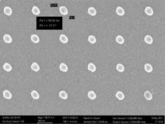
SEM images of tungsten nanodots deposited by EBID |
|
| |
Structures with various geometries have been fabricated through Electron beam assisted local etching (EBID) in PMMA and SiO2, using water and fluorine vapors as precursors. |
| |
| |
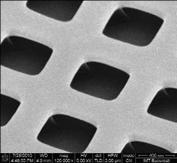
“Chessy-like” structure, composed of 1 micron squares (30 nm corner radius)
etched by EBIE process in PMMA using water vapor precursor
|
|
|
Right: Etched structure in SiO2 substrate by EBIE using fluorine precursor Left: detail |
Projects:
-
National basic funding Project MINASIST +, 2006-2008
-
FP7 project Carbon nAnotube Technology for High-speed nExt-geneRation nano-InterconNEcts – CATHERINE (FP7/STREP, 2008-2010) |
| |
- high aspect ratio structures at nm scale fabricated through EBL-based techniques |
| |
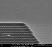
By proper tuning various EBL process parameters, we managed to obtain nanostructures with high aspect ratio (> 5:1) both in PMMA and SU8 electronresists.
|
|
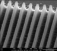
SEM micrographs of high aspect ratio (12:1) PMMA cross-lines , 125 nm pitch
a) top view; b) (450 tilt angle) |
|
|
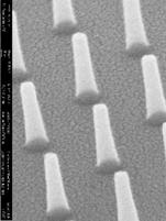
|
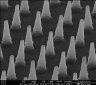
a) 45º tilted view |
b) top view |
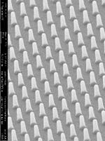
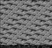
SEM micrographs of 2 μm height, high aspect ratio SU8 structures.
a) lines with 1/3 fill factor (aspect ratio 20:1) ; b) pillars (aspect ratio 6:1) |
|
| |
- aditive methods for fabrication of nano-interconections on various substrates: lift-off for metals and dielectrics by using special methods for exposure and treatment of electronresist, lithography with double layer etc. |
| |
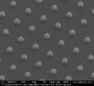
Additive methods - lift-off si EBID - have been used for transferring on different substrates nanometer configurations of dots and lines – basic elements of vertical and horizontal interconnects. The ultimate goal was to produce areas of metallic nanodots used as catalysts for vertical growth of carbon nanotubes and lines with less than 100 nm widths, intended as test structures for interconnection of two vertical beams of CNTs.
|
|
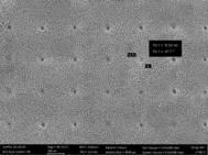
SEM micrographs of 18 nm diameter (left) and 79 nm diameter (right) holes in PMMA, fabricated by EBL |
|
|
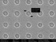
a) |
b) |
SEM micrographs of Ni dots (average diameter 80 nm) and lines
(100 nm medium width), fabricated using EBL and lift-off. |
|
| |
- fabrication of 2D and 3D nanostructures intended to be used as calibration gratings for optical microscopy, AFM and STM with better than 100 nm accuracy |
| |
|
|
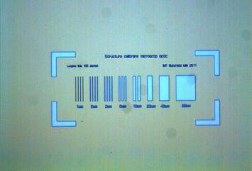
Calibration structure for optical microscopy fabricated using EBL. Linewidths: 1 μm to 80 μm
|
| |
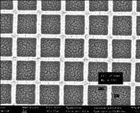
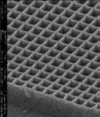
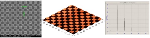
calibration grid with periodic1 µm pitch squares, fabricated by EBL
- SEM (a) and AFM (b) images (c) Power spectrum of the Fourier transform of the image in b) |
Project: National basic funding Project CONVERT +, PN II - (2009-2011)
Contact person: Dr. Adrian Dinescu e-mail:adrian.dinescu@imt.ro |
| |
|
|
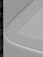
Suspended PMMA structures for photonic applications |
3D patterning of PMMA 35K |
|
|
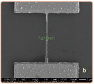
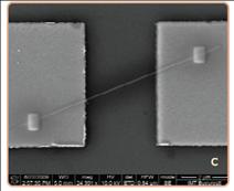
Calibration structure for high frequency measurements on CNts |
Carbon nanotube fixed in place using EBID (Electron Beam Induced Deposition) |
|
| |
Nanolithography with sub 20 nm resolution;
• Three-dimensional nanostructures;
• CNT based interconnections for next-generation
integrated circuits
• CNT based nanodevices
• SAW devices with nanometer interdigitated
electrodes;
• Optical devices, holograms, micro lenses, gratings
• Development of Nanodevices using E-beam induced
deposition and etching
• Development of circuits for communications based
on photonic crystals
Contact person: Dr. Adrian Dinescu e-mail:adrian.dinescu@imt.ro |