¤ Results
Expected results:
Scientific results:
- New technology for a piezoelectric MEMS Harvester to be used for powering biomedical devices or Sensor Networks
- Simulation results of Piezoelectric harvester for several designs and optimisation for high energy harvesting
- Simulation and Design of MEMS harvester device to be used in several applications and providing different power supply.
- The technology and the prototype of piezoelectric harvester including storage and compensation electronics tested in real environment applications
Other proposal related results:
- Patents to be transferred to the end-users or users in order to take advantage of the above results for business purposes.
- Increasing of international cooperation, working in a multidisciplinary field
- Contribution to: green energy field development, reduction of CO2 emissions, improving the quality of life for elderly patients and general population, reduction of energy costs.
Concept:
The concept of the project related to multiple MEMS piezostructures integrated with the storage module is presented in the figure below. Two rows with 10 cantilevers each will be integrated. They will be electrical connected in such a way to collect all harvested energy in a unique storage module. The full module will have 1 cm x 1 cm dimensions and will provide 100 uW / mm3 or more.
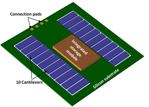
The piezoelectric beam array, consisting of two rows of 10 cantilevers each
with a median area for storage and power circuitry
Results (under development):
Design, modelling and optimisation of the Piezo-MEMS device
Several different geometric and/or structural versions of the cantilever were defined and analyzed, with the purpose to determine the most suitable one in terms of principal vibration modes (especially for the bio-medical applications, the harvester needs to run at low resonant frequencies).
The first step was to deploy a modal analysis, to determine the principal vibration modes of the cantilever.
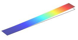 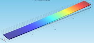
The main vibration mode (flexure fundamental) for the polysilicon-based cantilever (left) and the Si-based cantilever (right)
Next, analyses were directed towards finding the optimum dimensions for the cantilevers. The length was varied between 500 and 2,500 µm, the width was tested within the 150 – 500 µm, while maintaining a regular ratio of 1/5 to 1/10. The optimum pair of dimensions was found to be 2,500 /300 µm.
The last step was to add and optimize an inertial mass for the Si-based device, in order to increase its deflection and reduce the resonant frequency. It was added towards the free end of the cantilever and several geometric parameters were targeted for optimization purposes:
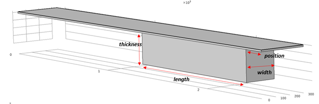
Inertial mass geometric optimisation
The optimum values of the inertial mass parameters:
- Length: 1,200 µm;
- Width: 300 µm (equal to the cantilever’s width);
- Thickness: 400 µm;
- Position towards the beam end: 0 µm.
The resonant frequency for the optimized geometry: 404 Hz (approx. 4 times lower than the simple Si beam version. The inertial mass weight is 3.35E-7 kg.
Technological development
We made several tests for the KNN and silicon etching. The KNN layers were fabricated on Pt/TiO2 substrate by Jožef Stefan Institut from Ljubljana, Slovenia. A RIE (Reactive Ion Etching) process was used for the KNN etching. The etching was successful and the results are shown in the figure below.
Etched KNN

 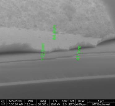
SEM image for dry etching of KNN layers
The silicon has been etched by a DRIE (Deep Reactive Ion Etching) process on 3” wafers with a <100> orientation. In this case the layers consists in Si3N4/SiO2/Si. The results are shown in the figures below.
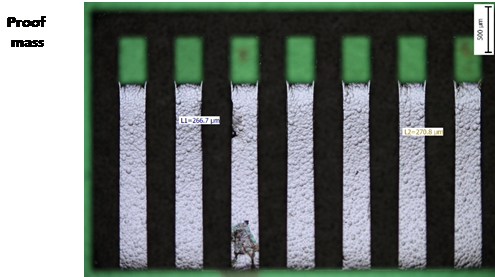
Cantilevers release by DRIE etching (back of the wafer)
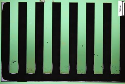
Cantilevers release by DRIE etching (front of the wafer)
[Home page]
|