
Welcome to SAWSAT website!
GaN/Si Lumped-Element SAW Duplexers for Satellite Telecommunications above 7 GHz
Project type: Experimental Demonstrative Project
Project duration: 23.10.2020-22.10.2022
Project budget: 584.950 RON
Domain project: INFORMATION AND COMMUNICATION TECHNOLOGIES, SPACE AND SECURITY

Results 2022
The third stage of the SAWSAT project corresponds to Task 3.1. Characterization of SAW band pass filters (Run 2); Task 3.2. SAW resonator duplexer specifications; Task 3.3. Design of SAW resonator duplexer; Task 3.4. Fabrication of SAW resonator duplexer (Run 3) and Task 3.5. Measurement and characterization of SAW resonator duplexer demonstrator (Run 3).
The main results obtained during the last stage of the project are related to the characterization of the SAW band pass filters designed in the previous stage and the modeling, design, fabrication and characterization of the SAW resonator duplexer demonstrators.
The band pass filter with 130 nm wide interdigital transducers (IDTs) showed insertion losses around 13 dB and reflection losses of 10 dB at 8.06 GHz, with a -3dB frequency bandwidth of 20 MHz and a maximum rejection (compared to the minimum insertion losses) of 30 dB at 8.15 GHz. The extracted quality factor is 344 and the effective electromechanical coupling factor is 0.1%.
A dedicated measurement setup was used to estimate the temperature effect in the – 55 °C ... + 125 °C range on the filter characteristic. The resulting thermal coefficient with frequency (TCF) is – 12 ppm/ °C which results in a maximum frequency shift of ±10 MHz for the central operating frequency. The circuit maintains its functionality. These results were reported at the European Microwave Conference held during the European Microwave Week, held in London in April 2022.
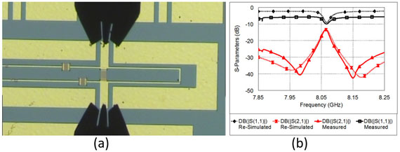
SAW band pass filter characterization: (a) fabricated device under test; (b) comparison between simulated and measured results [A.C. Bunea et al., EuMW, April 2022]
Due to the very small coupling coefficient, which directly influences the filter frequency band and the roll off factor, a Sc0.3Al0.7N piezoelectric thin layer deposited on high-resistivity silicon substrate was used for the fabrication of the duplexer circuits.
Based on experimental and simulation results, a set of specifications was defined for the surface acoustic wave resonator duplexer. These are: operating frequencies above 7 GHz and above 8 GHz for the two outputs, - 3 dB frequency bandwidths of at least 50 MHz, insertion losses lower than 23 dB and out-of-band rejection of 50 dB.
The duplexer circuit was designed based on face-to-face SAW transducer configuration, in order to obtain a much smaller circuit layout area. The inductive lumped elements (metallic strips) are placed in series with the input and the two outputs.
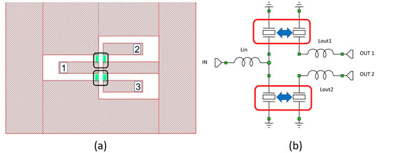
Duplexer circuit topology: (a) equivalent circuit; (b) circuit layout [A.C. Bunea et al., IEEE CAS, 2022].
The resonators are fabricated on a 500 nm thick Sc0.3Al0.7N layer deposited through pulsed laser deposition (PLD) technique (Solmates B.V.) on a 100 nm thick SiO2 layer, obtained through thermal oxidation on a 525 μm thick high-resistivity (>10000 Ohm·cm) silicon wafer. The two filters consist of interdigital transducers with 160 nm (simulated resonance frequency of 8.095 GHz) and 180 nm (simulated resonance frequency of 7.275 GHz) widths. These frequencies are in the target bands of the duplexer, namely 7.25-7.75 GHz and 7.9-8.4 GHz, respectively. Interdigital transducers of 140 nm (simulated resonance frequency of 9.2 GHz) were also selected for the fabrication of the experimental demonstrators.
The duplexer circuits were fabricated using a combination of nanolithographic and photolithographic technological processes. The interdigital transducer metallization is 5/45 Ti/Au and the surrounding circuit is 5/300 nm Ti/Au. The functional area of the circuit is represented by the four SAW resonators and is only 100 × 260 μm2, while the whole circuit is 1800 × 1250 μm2.
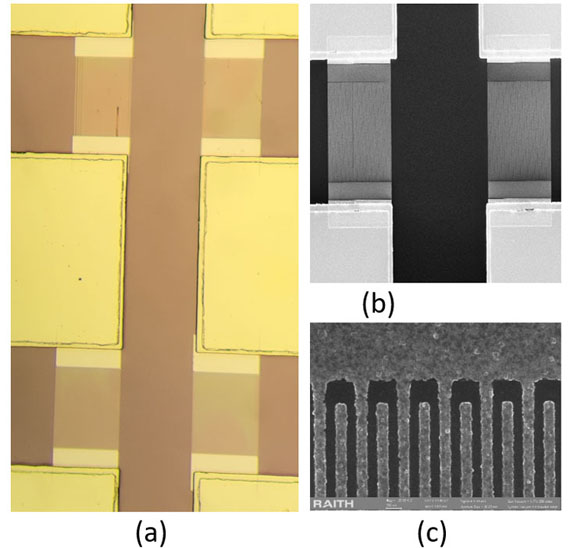
Example of fabricated duplexer circuit: (a) functional area of the duplexer circuit of only 100 × 260 μm2; (b) scanning electron microscope image of two face-to-face IDTs; (c) detail of nanometric IDTs
A dedicated method for the extraction of the 3-port S-parameters using 2-port measurements was developed for the characterization of the SAW duplexer circuits with 140 nm, 160 nm and 180 nm IDTs [A.C. Bunea et al., IEEE CAS 2022]. Operating frequencies of 7.5 GHz, 8.7 GHz and 9.9 GHz were obtained, with good channel definition for the different outputs, – 3dB frequency bandwidths of about 100 MHz and isolation between channels better than 40 dB.
All objectives of the 3nd Stage of the project were successfully accomplished.