I Results 2019 I Results 2018 I Results 2017 I
Title: Investigation of superior propagation modes in GHz operating GaN based SAW devices targeting high performance sensors and advanced communication system applications
Acronym: SupraGaN
Contract No: 147/2017 Project manager: Dr. Alexnadru Müller (IMT Bucharest)
Results obtained in 2019 (up to September 2019)
Third stage: investigation of pressure and temperature sensors based on Lamb propagation mode; parallel with similar SAW sensors based on Rayleigh propagation mode, k2eff vs. hk analysis and an exploratory study of filter type (face-to-face) SAW structures based on Sezawa and Lamb propagation mode
1. GaN membranes manufacturing and structures fabrication
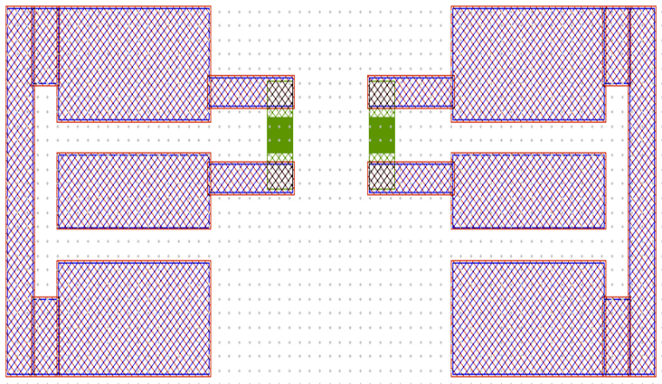
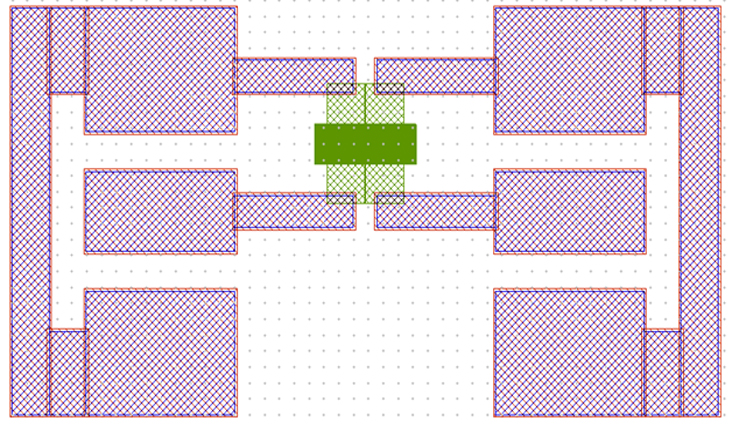
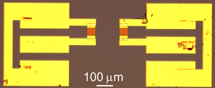
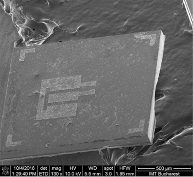
In the third stage of the SUPRAGAN project “face-to-face” SAW structures have been obtained on GaN commercial wafers from NTT AT Japan. The SAW structures were obtained using the electron beam lithography, an "e-line" equipement from Raith Gmb: interdigitated transducers (IDT”s) having 150 digiti and 50 reflectors and a length of 50 μm, metallized with 5 nm/95 nm Ti/Au layer have been obtained.
The masks design for “face-to-face” SAW have used the dedicated soft were CleWin and have been obtained in IMT with the DWL 66 equipment.
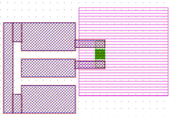
The superposition of the 4 masks is presented in figure 1
 |
Fig.1. Lay-out of the “face-to-face” SAW structures on GaN membrane (500 μm x 500 μm area and 1,2 μm thickness) |
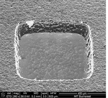
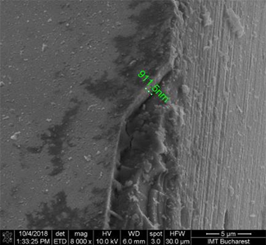
SEM images of the “face-to-face” SAW structure on GaN membrane (500 μm x 500 μm area) are presented in fig.2
 |
 |
(a) |
(b) |
 |
|
(c) |
|
Fig.2 SEM images of the “face-to-face” SAW structure on GaN membrane having 500 μm x 500 μm area and digit/inrertdigit width of 170 nm: (a) front image; (b)back-side image; imagini de pe spatele structurii; (c)oblique backside image |
|
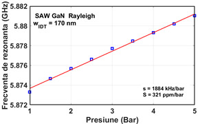
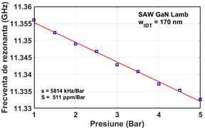
2. Parallel between Lamb and Rayleigh propagation mode for the pressure sensor
Measurements of the Sensitivity vs pressure at room temperature for SAW test structures on GaN membranes have been performed.
SAW structures suspended on GaN membrane with 500 μm x 500 μm aria and 170 nm digit/interdigit space have been analysed for Rayleigh and Lamb propagation modes.
It has been observed that the resonance frequency is rising with pressure for the Rayleigh mode (Fig.1.a). Using the linear approximation of resonance frequency variation with the pressure, a value of 321 ppm/Bar for the Sensitivity has been obtained.
 |
 |
(a) |
(b) |
Fig 3. Resonance frequency dependence with pressure for the SAW resonator on GaN membrane with 500 μm x 500 μm aria for Reyleigh mode (a); and for Lamb mode (b) |
|
3. Study of cuplling coefficient for GaN/SiC based devices
In the previous stages of the project, the cuplling coefficient (k2eff) of SAW structures on GaN/Si for Rayleigh and Sezawa modes as well as for the sructures on GaN membranes in Rayleigh and Sezawa modes have been studied and compared, now we have analysed the cuplling coefficient for SAW structures manufactured on GaN/SiC (Fig.2).
A comparaison for experimental obtained values of Rayleigh and Sezawa propagation modes has been performed.
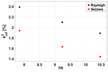 |
Fig.4 Parallel of experimental values of k2eff for Rayleigh and Sezawa modes of SAW structures on GaN/SiC |
For the cuplling coefficient (k2eff) study, SAW structures on GaN/SiC having the interdigitated traductor with space/interspace width of 150nm, 170nm and 200nm and 100nm metallisation have been used. From fig. 2, on observe that the cuplling coefficient values for Rayleigh mode are higher than the values measured in Sezawa mode.
4. Investigation of filter type structures (“face to face”) in superior propagation modes
For that objective, face to face SAW structures on GaN/Si have been analysed in order to emphasise the superior Sezawa propagation mode and face to face SAW structures on GaN membranes to emphasise the superior Lamb propagation mode.
4.1 Investigation of “face-to-face” SAW structure on Sezawa superior mode
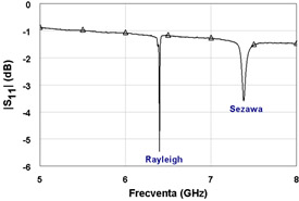
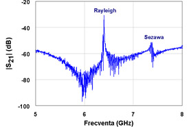
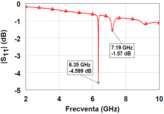
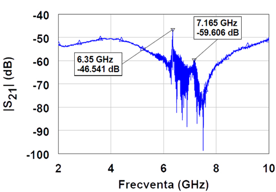
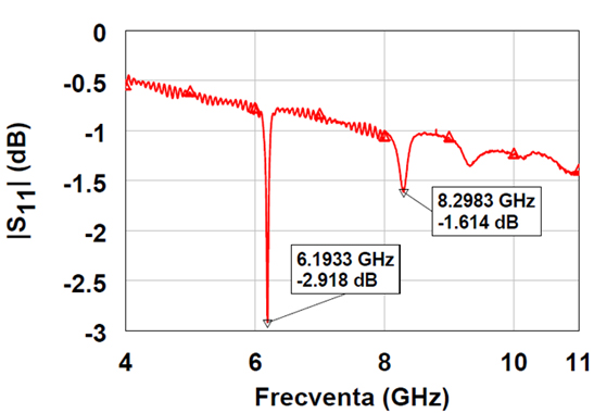
SAW structures face-to-face type having digit/interdigit width of 170nm on GaN/Si have been used. Refexion and transmission parameters are presented in fig.5.
 |
 |
(a) |
(b) |
Fig.5 Reflexion parameters (a)and transmission parameters (b) for a”face-to-face” SAW structure on ”o structura SAW de tip “face to face” on GaN/Si substrate |
|
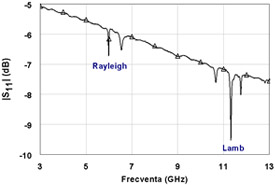
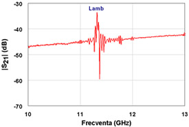
4.2. Investigation of “face-to-face” SAW structure on Lamb superior mode
The Lamb waves are generated in layers having the thickness ≤ the acoustic wave length using IDT’s [4].
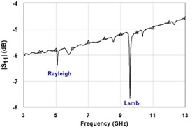
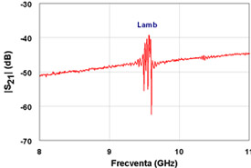
For this objective, face to face SAW structures on GaN membranes having digit/interdigit width of 170nm and respective 200nm. S11 and S21 measurements for these structures are presented in figure 6 and 7. The Lamb superior propagation mode is observed at 9.58 GHz, respective 11.32 GHz frequencies.
 |
 |
(a) |
(b) |
Fig.6 Reflexion parameters (a) and transmission (b) for a “face to face” SAW structure on a GaN membrane having digit/interdigit width of 200 nm |
|
 |
 |
(a) |
(b) |
Fig.7 Reflexion parameters (a) and transmission (b) for a “face to face” SAW structure on a GaN membrane having digit/interdigit width of 170 nm |
|
4.3. Supplementary project objective:
Measurements concerning a possible nonlinear behaviour of SAW structures for powers in the interval 0 – 20 dBm. The measurements and the results are in progress (authors:: Andrei Florescu, Sergiu Iordanescu).
Results obtained in 2018
Second stage: SAW temperature sensors on GaN/SiC based on Sezawa propagation mode investigation; comparison to the performances of similar SAW sensors based on Rayleigh propagation mode
1. Manufacturing and characterization of “face to face” type SAW structures based on GaN/SiC and GaN/Si
The “face to face” SAW structures have been manufactured on GaN/SiC and GaN/Si wafers from NTT AT Japan. The masks have been designed in CleWin dedicated software and have been manufactured in IMT with DWL 66 equipement. Masks layouts are presented in Fig 1.
 |
 |
(a) |
(b) |
Fig.1 Layout of “face-to-face” SAW structures manufactured on GaN/Si (a) and on GaN/SiC (b) |
|
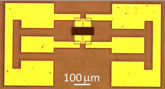
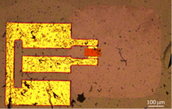
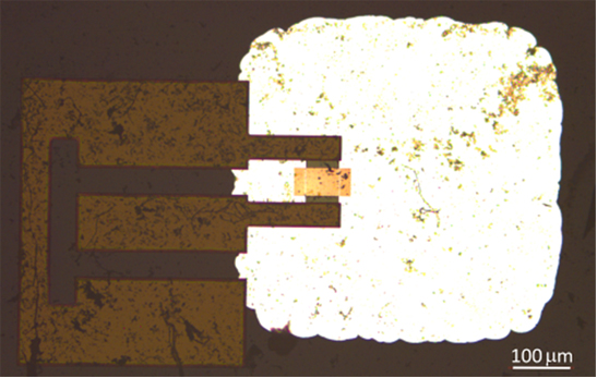
SAW structures on GaN/Si wafers with 170 nm digit/interdigit width and SAW structures on GaN/SiC with 150 and 170 nm width have been manufactured. Each IDT has 150 digits/interdigits with 50 μm length (Fig 2).
 |
 |
(a) |
(b) |
Fig.2 Photo of “face-to-face” type SAW structure: chip with CPW pads for GaN/Si (a) and GaN/SiC (b) |
|
The SAW structures have been characterized “on-wafer” with Anritsu Vector Network Analyzer 37397D and on-wafer set-up PM5 from Suss Microtec, using CPW pads. S11 and S21 parameters have been measured for three “face to face” SAW structures manufactured on GaN/Si and GaN/SiC wafers (Fig 3, 4).
 |
 |
(a) |
(b) |
Fig. 3 |S11| and |S21| for SAW face to face resonators on GaN/Si having IDTs 170 nm wide. |
|
 |
 |
(a) |
(b) |
Fig.4 |S11| and |S21| for SAW face to face resonators on GaN/Si having IDTs 170 nm wide |
|
Using the resonance frequency and the digit/interdigit width, the propagation velocity is calculated (Table 1).
Table 1. The calculated propagation velocity of the SAW structures on GaN/Si and GaN/SiC
Structure SAW |
w[nm] |
hAu [nm] |
hk |
vR [m/s] |
vS [m/s] |
GaN/Si |
170 |
100 |
9.24 |
4318 |
4889 |
GaN/SiC |
170 |
100 |
9.24 |
4209 |
5637 |
GaN/SiC |
150 |
100 |
10.47 |
4116 |
5406 |
2. Simulations of the mode shapes for SAW resonators manufactured on GaN/SiC
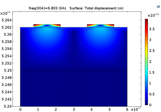
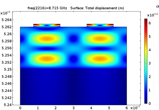
The numerical analysis was performed in COMSOL Multiphysics on 2D periodic models with the width of a wavelength (λ = 4w, w being the electrodes width), for SAW structures with different width of digits and interdigits: 200 nm, 170 nm, 150 nm. In Fig. 5 are presented the simulation results for the SAW structure with IDT having digits/interdigits spaces of 150 nm width. The resonance frequency corresponding to Rayleigh propagation mode is 6.8 GHz and for Sezawa mode the resonance occurs at 8.71 GHz.
 |
 |
(a) |
(b) |
Fig. 5 The mode shapes of the resonance frequencies for the SAW structure with IDT having w=150 nm and hAu=100nm, Rayleigh mode (a) and Sezawa mode (b) |
|
Table 2 – The resonance frequency extracted from simulations and experiment for the SAW structures on GaN/SiC
digit/interdigit width [nm] |
Rayleigh propagation mode |
Sezawa propagation mode |
||||||
fR sim. [GHz] |
vR [m/s] sim. |
fR exp. [GHz] |
vR [m/s] exp. |
fS sim. [GHz] |
vS [m/s] sim. |
fS exp. [GHz] |
vS [m/s] exp. |
|
200 |
5.45 |
4360 |
5.43 |
4351 |
7.36 |
5888 |
7.42 |
5938 |
170 |
6.16 |
4189 |
6.21 |
4227 |
8.07 |
5488 |
8.25 |
5614 |
150 |
6.8 |
4080 |
6.9 |
4150 |
8.71 |
5226 |
9.14 |
5489 |
3. SAW temperature sensor based on Sezawa propagation mode, manufactured on GaN/Si and GaN/SiC
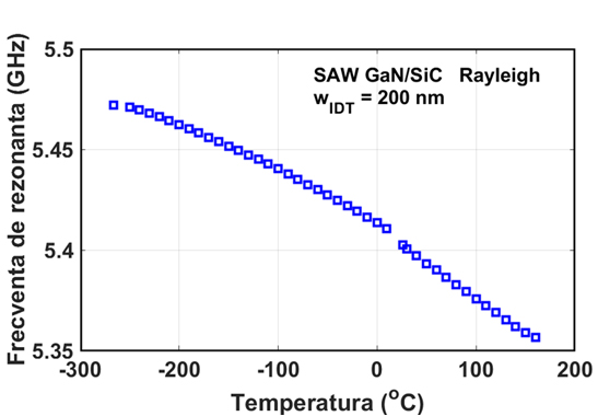
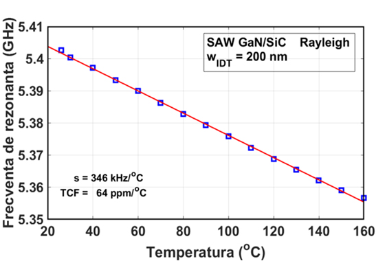
The temperature dependence of the resonance frequency (Rayleigh mode) of the SAW structures on GaN/SiC (digit/interdigit of 200 nm) was measured in the -266°C to 160°C range. The sensitivity of 346 kHz/°C has been extracted.
 |
 |
(a) |
(b) |
Fig. 6 The temperature dependence of the resonance frequency (Rayleigh mode) in the |
|
For the Sezawa mode, the temperature measurements have been performedin two temperature intervals: -266°C to 26°C and 26°C to 160°C (Fig 7). For the second interval, the dependence of resonance frequency with temperature is linear. For temperatures under 250°C (23 K), the structures are insensitive with temperature, which is very interesting for some modern applications, in the cryogenic temperature range.
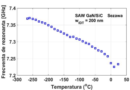 |
Fig. 7 The resonance frequency dependence with temperature in Sezawa mode, for -266°C to 26°C temp range |
For the temperature range 23°C - 150°C, the SAW resonance frequency variation has been measured for both wafer type, having digit/interdigit width of 150 nm and 170 nm, inside a cryostat. For the structures on GaN/Si we have obtained for the sensitivity s ~ 500 kHz/°C,and for the structures on GaN/SiC the sensitivity s~ 400 kHz/°C for Sezawa propagation mode.
4. GaN membrane and test structures manufacturing
For this type of structures, GaN/Si wafers from NTT AT Japan have been used. The layout and the SEM images of the structures are presented in figure 8.
 |
 |
 |
(a) |
(b) |
(c) |
Fig. 8 SAW structures on GaN membrane of 1,2 μm thin and 500 μm x 500 μm membrane area (a) SAW layout; (b) photo image – top view; (c) photo image – backside view |
||
 |
 |
 |
(a) |
(b) |
(c) |
Fig.9 SEM images of the SAW structure having 500 μm x 500 μm membrane area: (a)SEM image-top view; (b) GaN membrane of 1 μm; (c) SEM image - backside view of the membrane |
||
The manufactured SAW structures have been characterized measuring the reflection coefficient S11 with the Vector Network Analyzer (Fig. 10).
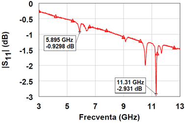 |
Fig. 10 |S11| parameter for the SAW structure manufactured on GaN membrane for digit/interdigit width/space of 170 nm |
Table 3. The calculated values of the propagation velocity in SAW structures on GaN membranes
w[nm] |
hAu [nm] |
hk |
vR [m/s] |
VL [m/s] |
300 |
80 |
5.23 |
4008 |
7728 |
200 |
80 |
7.85 |
4048 |
7704 |
170 |
80 |
9.24 |
3991 |
7718 |
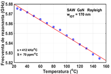
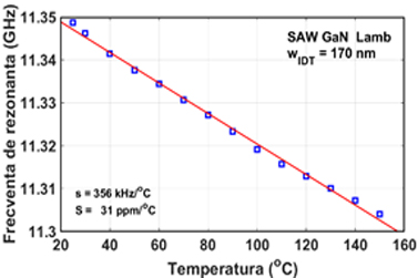
5. Parallel between Lamb and Sezawa propagation mode for the temperature senzor
The temperature sensor developed on GaN membrane supported SAW structure is based on two propagation modes: Rayleigh and Lamb.
 |
 |
(a) |
(b) |
Fig.11 Resonance frequency dependence with temperature for (a) Rayleigh mode and (b)Lamb mode for the SAW resonator on GaN membrane with 500 μm x 500 μm area |
|
For the Rayleigh mode we have obtained TCF = 70 ppm/°C (Fig. 12a); for Lamb propagation mode we have obtained TCF= 31 ppm/°C. The Rayleigh mode has higher sensitivity with temperature then the Lamb mode.
Results obtained in 2017
Contract No: 147⁄2017
Proiect: Investigation of superior propagation modes in GHz operating GaN based SAW devices targeting high performance sensors and advanced communication system applications - SupraGaN
First stage: Investigation of Sezawa propagation mode on SAW devices working in GHz frequency range, manufactured on GaN/Si and GaN/SiC
1. Manufacturing and characterization of the single SAW resonator structures realized on GaN/SiC and GaN/Si
Single SAW resonator structures were manufactured on GaN/SiC and GaN/Si wafers purchased from the NTT AT Japan. The GaN layer was grown by Metal-Organic Chemical Vapor Deposition (MOCVD) on both SiC substrate with high resistivity (> 105 W·cm) and crystallographic orientation (0001), and respectively on Si substrate with a resistivity higher than 6000 W·cm and crystallographic orientation (111). A buffer layer with a total thickness of 0.2 μm was grown between the Si substrate and the 1 μm thin undoped GaN layer.
The masks have been designed for different SAW structures using the dedicated program CleWin. The masks were manufactured at IMT Bucharest, on the DWL 66 equipment. The superposition of the three designed masks is shown in Fig. 1 (a).
Once the technological processes were achieved, the structures were morphologically characterized by the Scanning Electron Microscope - Vega II LMU (TESCAN). Figure 1 (b) shows the SEM image of a SAW structure manufactured on GaN/Si wafers having a digit/interdigit width of 200 nm and a length of 100 μm.
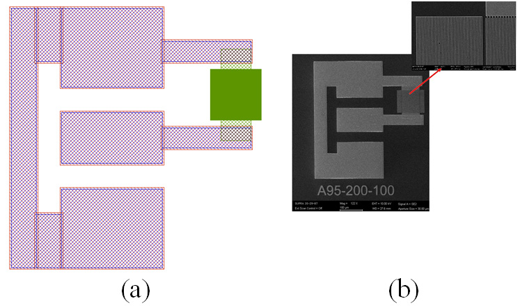 |
Fig. 1 (a) Layout of the single SAW resonator structure (b) SEM photo of the SAW: chip with coplanar waveguide type pads; the inset presents a detail of the nanolithographic process |
1.2. Analysis of the Sezawa propagation mode
In order to achieve the main objective of this stage, the Sezawa propagation mode that appears in SAW structures manufactured on thin GaN layers grown on SiC and Si substrates have been analyzed.
1.2.1. Analysis of the Sezawa mode in GaN/SiC structures
Single SAW resonator structures were manufactured on 1 μm thin GaN layer grown on a SiC substrate. Three types of SAW structures with interdigital transducers (IDTs) having finger/interdigit width/spacing of 200 nm, 170 nm and 150 nm, and 100 nm thin Au metallization were fabricated and analyzed.
Considering the values of the Rayleigh mode velocity as well as the values of the transverse velocity in Si and GaN, shown in Figure 2 through a dotted line, the three resonances can be associated to the Rayleigh (R), Sezawa (S) and Pseudo-Bulk (PB) modes. Fig. 2 shows the variation of the propagation velocity for the three modes, depending on the normal thickness of the GaN layer grown on the SiC substrate, for the three types of SAW structures.
The experimental values of the acoustic velocity vs. normalized thickness, hk, were analyzed for the Sezawa mode and compared to those for the Rayleigh and pseudo-bulk modes. Sezawa mode resonances having acoustic velocities with approx. 30% higher than the Rayleigh mode have been obtained. For the Sezawa mode, the acoustic velocity decreases monotonically with the increase of hk.
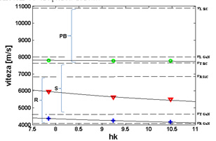 |
Fig. 2 Acoustic velocity vs. the normalized thickness for all three SAW test structures |
1.2.2 Analysis of the Sezawa mode in GaN/Si structures
Single SAW resonators were fabricated on a GaN/Si wafer having the thickness of the GaN layer 1 μm. In order to obtain a wide range of hk, SAW resonators with IDT having the width/spacing of the finger/interdigit 200, 170, 150, and 120 nm have been manufactured. For all these SAW structures, the metallization of the IDT was 100 nm. Also, SAW structures with IDT having the finger/interdigit width of 200 nm and metallization of 50 nm have been analyzed.
Fig. 3 shows the experimental values the acoustic velocity vs. hk of the GaN layer, for all five types of SAW resonators and all three propagation modes. A monotonic decrease of the acoustic velocity with the increase of the hk was observed for the Sezawa mode. Acoustic velocity values approx. 15% higher than Rayleigh mode have been obtained for the Sezawa mode.
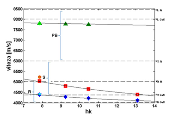 |
Fig. 3 Acoustic velocity vs. the normalized thickness for SAW structures with 100 nm thin metallization (dark colors) and for SAWs with 50 nm thin metallization (light colors) |
2.Simulations of the mode shapes for SAW resonators on GaN/Si
The numerical analysis was performed in COMSOL Multiphysics on 2D periodic models with the width of a wavelength (λ = 4w, w being the electrodes width). Figure 4 represents the admittance module vs. the frequency for the SAW structure with IDT having digit / interdigitated spacing width 120 nm and 100 nm Au metallization thickness. Two resonances were obtained corresponding to Rayleigh propagation (f = 8.7 GHz) and Sezawa mode (f = 9.26 GHz). The corresponding waveforms are shown in Fig. 5. For the Rayleigh mode the displacement has the maximum value in the electrodes and in the GaN layer. In the case of the Sezawa propagation mode, the maximum displacement is inside the electrodes and in the GaN layer, penetrating into the Si substrate 0.3 μm.
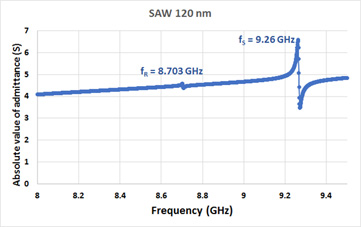 |
Fig. 4 Absolute value of the admittance for the SAW structure having IDT with w=120 nm and hAu=100nm |
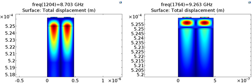 |
Fig. 5 Simulated mode shapes for the SAW structure with IDT having w=120 nm and hAu=100nm (a) Rayleigh mode; (b) Sezawa mode |
The simulated resonance frequencies (R) and (S) are very closed to the experimental results, (estimated error between 0.5% and 2%). A comparison between the resonance frequencies extracted from simulation and experiment are presented in Tabel 1.
Table 1 – The resonance frequency extracted from simulations and experiment for the SAW structures on GaN/Si
Digit/ interdigit spacing width [nm] |
Metallization thickness [nm] |
Rayleigh propagation mode |
Sezawa propagation mode |
||
Simulated resonance frequency [GHz] |
Experimental resonance frequency [GHz] |
Simulated resonance frequency [GHz] |
Experimental resonance frequency [GHz] |
||
200 |
100 |
5.52 |
5.48 |
6.42 |
6.3 |
50 |
5.56 |
5.51 |
6.52 |
6.52 |
|
170 |
100 |
6.25 |
6.29 |
7.14 |
7.06 |
150 |
100 |
6.996 |
7.03 |
7.72 |
7.76 |
120 |
100 |
8.703 |
8.56 |
9.263 |
9.3 |