DIP PEN NANOLITHOGRAPHY SYSTEM NScriptor 2008
Is a nanolithography system that „prints” and „ink” directly on the substrate. The size of the geometrical features can vary from few tens of nanometers (in best conditions – 20 nm) up to several microns. It allows both a bottom-up approach and a top-down one when contructing the nanostructures. The working principle is that of wetting an AFM-type cantilever with an “ink” and writing down onto a substrate, similar with an ink pen that writes on a paper. The process is serial and is quite slow, but can be highly parallelized by using 2D arrays of cantilevers (55,000 such cantilevers on an array) and thus becomes efficient from the speed and throughoutput points of view. Many materials can be used as “inks”, as are solutions of polymers, small organic molecules, sol-gel precursors, macromolecules, nanoparticle colloids.
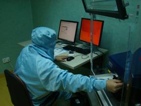
Seting-up the system. Left monitor: used for working with the CAD-like software that controols the system; right monitor (orange): real-time imaging of the cantilever tip; extreme right (blue): the NScriptorTM system. The window of the environmental chamber is open.
Performance:
- minimum width: 15 nm resolution on single crystal surfaces, < 50 nm on polycrystalline surfaces
- minimum separation between adiacent lines: 5 nm
- positioning accuracy: + / - 2 nm
- maximum length of a line: 85 microns
Materials used:
- substrates: metals (Au, Pt, Al, Ni), SiOx, SiO2, Si, Ge, GaAs, mica and others;
- materials that can be deposited : Thiols, Silanes, Silazanes, Alkynes, Cystamine, Sol-Gels;
Nanoparticles colloids (metal, Silicon), Catalysts, Metal Nanoclusters, DNA, proteins, biomolecules, Carbon Nanotubes, polymers, organic molecules (small, medium and large)
Below is the acronym of the National Institute of Microtechnology – Bucharest written at the nanoscale, by using the system:
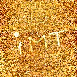
Image size is 5 microns x 5 microns, the width of the letters is 115 nm while the dot radius on top of letter “i” is 180 nm. Written with an organic acid (MHA) on gold substrate. Image was read by Atomic Force Microscopy at angle of 100 with respect to the writing direction.
Some examples of applications of the dip pen nanolithography technique are presented below:
- surface functionalization (with direct liaison to proteomics, DNA recognition, virus identification);
- photolithographic masks correction;
- molecular electronics;
- realization of master stamps for NIL (Nanoimprint lithography)
- novel devices (photonic and electronic);