
Welcome to EgiDe website!
Engineering low dimensional heterostructures for boosting the performances of on-chip 3D energy storage / power delivery device
Project duration: January 04, 2021 - December 31, 2023
Project budget: RON
Domain project: Physical sciences and engineering
Results
Stage 3, Fabrication of 3D nanostructured MSC test devices, 2023
____________
Stage 2 - 2022 Fabrication of preliminary test assemblies based on novel heterostructures
The proposed objectives and tasks in this stage were achieved as follows:
Task 2.1 Three types of nanostructured substrates where proposed: i) porous silicon (pSi), ii) silicon nanowires (SiNWs), and iii) vertical graphene nano-walls (VGNWs) for which an ultrathin layer of titanium nitride (TiN) or vanadium oxide (V2Ox) was coated on their surface or a polymer which were subsequently graphitized. These novel heterostructures were further subjected to morpho-structural characterization by SEM and XRD and compositional analysis by XPS the focus being assessing the presence of the thin films on their surface and their crystallization state. The SEM micrographs of the unmodified/modified heterostructures could be found in Fig. 1, where both top and cross-sectional views are depicted. In the first two columns could be seen the unmodified heterostructures: a) vertical graphene nano-walls (a), silicon nanowires (e), porous silicon (i), and their cross-sectional views: (b), (f), (j). The last two columns were reserved for the modified heterostructures (c), (g), (k) and (d), (h), (l) respectively.
 |
Figure 1: SEM micrographs of fabricated heterostructures: a) VGNWs (top view); (b) VGNWs (cross section), (c) VGNWs coated with a thin layer of V2O5; (d) VGNWs coated with a thin layer of TiN, (e) SiNWs (cross sectional view); (f) SiNWs (in between top and cross section, 45 deg); (g) SiNWs coated with V2O5; (h) SiNWs coated with TiN, (i) cross sectional view of graphitized pSi (pSi-G); (j) pSi-G coated with TiN (cross sectional view); (k) pSi-G (top view) si (l) pSi-G coated with TiN (top view). |
Even though the micrographs from Fig. 1 clearly shows the presence of the thin layers on the heterostructures’ surface, several analyses were conducted to further verify if it is the material coated on top or just some possible artefacts due to the very small thickness of the films or even the reaction products that were not rinsed. Both XPS and XRD analyses assess the presence of the films on top of the hybrid architectures. More specifically, for the samples containing vanadium oxide deposited on SiNWs and VGNWs, XPS showed a mixture of V2O5 and VO2 phases.
Task 2.2 Three types of electrolytes were tested and one encapsulation method was proposed of the on-chip implementation of supercapacitors. The difficulty of assembly a supercapacitor that works on aqueous electrolytes was overcome by a FDM (fused deposition method) 3D in- house printed system (showed in Fig. 2).
 |
Figure 2: (a) Assembly layout; (b-d) Different views of assembled supercapacitor using our in-house system. |
In fig. 2 (a) is depicted a simplified schematics of the layout with all dimensions. A gasket was used to prevent the loss of electrolyte in the assembly process, moreover silicon-based lubes (non-conductive) were also used to enhance the sealing. The distance between the two electrodes was 100 ![]() which could be tuned by modifying the depth of gasket groove (dark grey) (it is very hard to obtain a constant separation due to the non-uniformities of the gasket) or by modifying the depth of the electrode groove (neutral grey). A carbon-based lube was used to increase the quality of the back contacts. The electrodes were fabricated by coating 5 nm of Chromium as adhesion layer and 300 nm of Gold on low resistivity Silicon wafer (0.001- 0.005
which could be tuned by modifying the depth of gasket groove (dark grey) (it is very hard to obtain a constant separation due to the non-uniformities of the gasket) or by modifying the depth of the electrode groove (neutral grey). A carbon-based lube was used to increase the quality of the back contacts. The electrodes were fabricated by coating 5 nm of Chromium as adhesion layer and 300 nm of Gold on low resistivity Silicon wafer (0.001- 0.005 ![]() ).
).
Task 2.3: The fabricated test-structures where electrochemically characterized by employing the classical three electrode measurements such as cyclic voltammetry (CV), galvanostatic charge discharge (C&D) and electrochemical impedance spectroscopy (EIS). In addition, a more advanced technique based on Scanning Electrochemical Microscopy (SECM) was also considered. The SECM analysis were performed on the TiN modified pSi-G samples, where the film thickness varies from 20 to 70 nm. By a direct comparison of experimental measurements with the theoretical model, the heterogenous reaction rate could be found from the following formula: ![]() . If the electrode radius (
. If the electrode radius (![]() ) and the redox mediator’ diffusion coefficient (
) and the redox mediator’ diffusion coefficient (![]() ) are known, the I order heterogenous reaction rate (
) are known, the I order heterogenous reaction rate (![]() ) could be computed. Using the aforementioned formula and plugging
) could be computed. Using the aforementioned formula and plugging![]() , and
, and ![]() = 5
= 5 ![]()
![]() which represend the diffusion coefficient of aqueous solution of Ru(NH3)6Cl2 2mM,
which represend the diffusion coefficient of aqueous solution of Ru(NH3)6Cl2 2mM, ![]() was obtained for all the TiN layer thicknesses. The results could be found in Table 1.
was obtained for all the TiN layer thicknesses. The results could be found in Table 1.
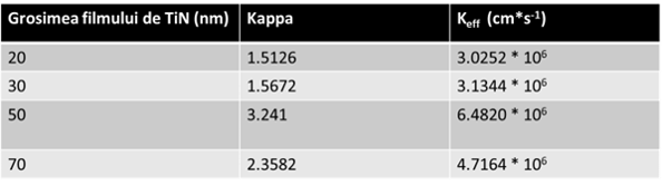 |
Based on the values from Table 1, in the normal conditions and unpolarized pSi-G substrate (![]() ) the sample of pSi-G coated with 50 nm TiN layer exhibited the highest electrochemical reactivity among the other TiN thicknesses.
) the sample of pSi-G coated with 50 nm TiN layer exhibited the highest electrochemical reactivity among the other TiN thicknesses.
In order to test the proposed configurations capabilities as electrodes for supercapacitors and to assess their electrical performances, three electrolytes were used: i) sodium sulfate, Na2SO4, ii) sulfuric acid H2SO4, and iii) a lithium based one LiClO4. To asses properly the performances of each configuration (electrolyte/TiN thickness), the capacitance was computed over the discharge zone (quadrant 2 and 4 from Fig. 3) and compared in absolute value for each electrolyte and TiN thickness. In the second quadrant where the supercapacitor discharges from the maximum positive potential to 0 V with a linear descending potential as in the classical cyclic voltammetry analysis (first column of Fig. 3) shows that the Na2SO4 configuration exhibited the highest capacitance for TiN layer thickness of 30, 20, and 70 nm, followed by LiClO4 for TiN thicknesses of 20, 30, 70 nm.
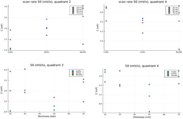 |
Fig.3: The computed capacitance from the classical cyclic voltammetry for all configurations |
By further analyzing the both quadrants (the second one and the fourth one) from Fig. 3, it can be seen that on the positive region (second quadrant) the sulfuric acid exhibited the lowest capacitance whilst the sodium sulfide shows the highest coulombic efficiency even though it reached oxidation on charging. In the second quadrant the 30 nm TiN electrode displays a higher value of capacitance for both sodium sulfide and sulfuric acid in comparison with the lithium based one. Even though, LiClO4 also reached the supraoxidation region, its perfomances were situated in between sodium sulfide and sulfuric acid. The highest capacitance obtaned for a thickness of 70 nm of TiN, was exhibited by the LiClO4, the electrolyte showed an increase in oxidation greater than the other two, indicating that, it contributed more to the electrodes surface degradation. The fourth quadrant (negative region), the value of capactiances for all configurations were halved in comparison with the ones obtained in the positive region (second quadrant). In this region, the electrodues where discharged from the highest negative potential to 0 V, and capacitance was computed on discharge. Here we can obseved again, that the performances of LiClO4 are in between the other two electrolytes, but in this case, with a smaller difference to sulfuric acid from the point of view of maximum capactiance values. In comparison with the second quadrant, the electrolytes order is reversed.
We cannot talk about supercapacitors performances without considering the the charge discharge curves. In these measurments, the intensity was kept constant at a value of 50 ![]() A and the potential is displayed as function of the time required for a complete discharge. For an ideal capactior the charcteristic should be a straing line with negative slope, in the case of supercapacitors being a device that depends on potential, for each sample the characteristic exhibits a positive slope to the potential value which in CV corresponded to a maximum, thus indicating in that region that an active material is involved in a reaction, leading to a change in potential curve. In Fig. 4, the values of capacitances obtained from the discharge curve are displayed for each configuration of electrylyte and TiN thickness.
A and the potential is displayed as function of the time required for a complete discharge. For an ideal capactior the charcteristic should be a straing line with negative slope, in the case of supercapacitors being a device that depends on potential, for each sample the characteristic exhibits a positive slope to the potential value which in CV corresponded to a maximum, thus indicating in that region that an active material is involved in a reaction, leading to a change in potential curve. In Fig. 4, the values of capacitances obtained from the discharge curve are displayed for each configuration of electrylyte and TiN thickness.
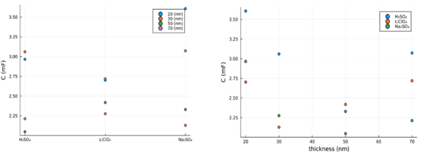 |
Fig.4: : The computed capacitance from the discharge curves for all configurations |
Therefore, the obtained results for each configuration of electrolyte and thickness of TiN were compared and discussed, from data analysis it was shown that the best electrolyte that leads to a good capacitive behavior is Na2SO4 for the electrodes coated with 30 nm TiN.
Results:
-
These results were reported in the following ISI scientific papers:
-
" Graphitized porous silicon decorated with cobalt hexacyanoferrate nanocubes as hybrid electrode for high-performance supercapacitors”, Irina-Nicoleta Bratosin, Cosmin Romanitan, Gabriel Craciun, Nikolay Djourelov, Mihaela Kusko, Marius C Stoian, Antonio Radoi, Electrochimica Acta (2022) Volume 424, 20 August 2022, 140632.
-
“X-ray scattering profiles: revealing the porosity gradient in porous silicon”, Cosmin Romanitan, Ioan Valentin Tudose, Kyriakos Mouratis, Marian Catalin Popescu, Cristina Pachiu, Stelios Couris, Emmanouel Koudoumas, Mirela Suchea, Physica Status Solidi A-Applications and Materials Science (2022) Volume219, Issue16, Article Number 2100431.
-
The obtained results were also presented at 4 ISI indexed scientific conferences (1 keynote presentation, 2 oral presentations, and 2 posters)
____________
Stage 1 - 2021
Activity 1. Design of MSC 3D architectures on silicon.
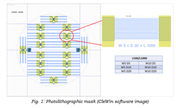
One of the project objectives is to find the optimal 3D architecture of the planar supercapacitors’ interdigitated structures. Therefore, we started with a standard interdigitated structure where, in order to understand how geometry influences the processes of storage / release and to carry out a systematic study in this regard, structures with two different lengths of digits, respectively 500 and 1000 µm, two widths of digits, respectively 5 and 10 µm µm, and three interdigit distances, respectively 5, 10, and 20 µm, were designed. Thus, 12 different configurations were finally designed on the photolithographic mask lay-out. To isolate the metal tracks, an additional mask was designed, which would leave only the active area free (detail image in Figure 1), allowing a correct analysis of the phenomena that take place in the system.
 |
Activity 2. Fabrication of original heterostructures interplaying capacitive-, pseudocapacitive- and battery-like nanomaterials.
Two alternatives for the fabrication of 3D planar structures will be followed:
1. Fabrication in a first stage of a 3D substrate with desired storage properties, followed by metallic interdigitated structure patterning in the second stage. The area between the digits will be corroded by a RIE process to allow the addition of the electrolyte.
2. The initial definition of interdigits followed by the deposition of the active material; In this case, the mask 2, for isolating the metal traces, is also helpful for the process of electrodeposition of the active compounds, which will be located on the metal digits.
2.1. For the first technological flow alternative, in which we first aim to obtain substrates that have supercapacitive properties, we systematically studied the influence of the porosity and thickness of the layers on the load storage properties. In this sense, p-type silicon wafers were porosified, 1-5 mΩ∙cm resistivity, (100) crystallographic orientation, with a diameter of 100 mm and a thickness of 450 μm, supplied by Siegert Wafer GmbH, by electrochemical corrosion in 1: 1 (v / v) electrolyte solution (40 wt.% HF and 98 wt.% ethanol) at different constant current densities: 10, 30, 50, 70, 90 and 110 mA/cm2. The process was repeated for two different time values, 5 minutes and 10 minutes, respectively, finally obtaining 12 types of electrodes with different degrees of porosity.
The electrochemical deposition of 7-hydroxy-1,2,3,4-tetrahydro-naphtalene-2-carboxylic acid on the silicon electrode through potentiometry was carried out using Autolab 302 N equipped with FRA 32 M, SCAN 250 and ADC 10 M modules, at a constant current density of 39 mA/cm2 for 120 s in a solution of 2 mM 7- hidroxy-1,2,3,4-tetrahidronaphtalene-2-carboxilic acid in 10 mM PBS and 0.1 M KCl serving as the electrolyte, with the porous silicon sample as the working electrode (WE), a saturated calomel electrode as the reference electrode (RE) and a Pt wire as the counter electrode (CE). The polymerized electrodes were cleaned with deionized water, dried under N2 and thermally treated at 800° C for 4h. Finally, the modified Si wafers were cut into rectangular pieces of 1.2 cm by 1.8 cm, and a symmetric plane parallel supercapacitor was assembled from each type of electrodes obtained, the two electrodes separated by a Meltonix gasket membrane and PVA/H2SO4 gel for the electrolyte.
SEM measurements were performed to assess the quality and the state of each porous layer formed – Figure 2.
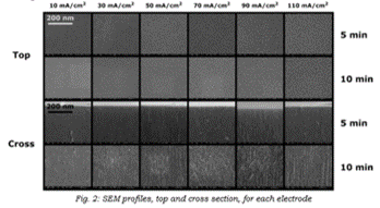 |
Looking at the top and cross sections above, we note that the pores are well defined and the paths are somewhat fractals, something which will be important when we’ll discuss the electrical behavior, since the pores distribution is a major influence when it comes to it.
First, CV measurements were performed for each symmetric plane parallel supercapacitor assembled at scan rates ranging over almost four orders of magnitude from 5 mV/s to 10 V/s and their voltammograms recorded at 50 mV/s scan rates were compared - Figure 3.
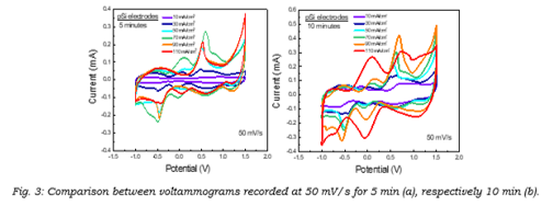 |
Figures 3 (a) and (b) show the resulting profiles from each electrode at 5 minutes and 10 minutes, respectively. Looking at the current values given by each electrode, we can draw a first conclusion that for 5 minutes, the electrode porosified at 70 mA/cm2 shows the highest current, while for 10 minutes it was the electrode obtained at 110 mA/ cm 2 current density. While the redox peaks suggest that the highest amount of polymer was deposited at 110 mA/cm2, they are not as well defined as is the case for 90 mA/cm2 or even for its 5 minutes counterpart.
More results can be found in papers:
"In-depth analysis of porous Si electrodes for supercapacitors”, Irina Bratosin*, Pericle Varasteanu, Cosmin Romanitan, Alexandru Bujor, Oana Tutunaru, Antonio Radoi, Mihaela Kusko*, The Journal of Physical Chemistry C(2021) 125, 11, 6043–6054.
“X-ray scattering profiles: revealing the porosity gradient in porous silicon”, Cosmin Romanitan*, Pericle Varasteanu, Dana C. Culita, Alexandru Bujor, Oana Tutunaru, Journal of Applied Crystallography (2021) 54, 847-855.
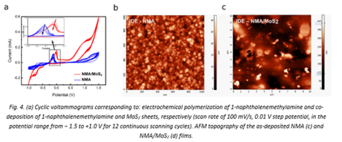
2.2. Preliminary experiments were performed to modify some electrodes interdigitated with nanomaterials; performance testing as supercapacitors. Thus, we tested the efficiency of the electrochemical deposition method for modifying interdigitated electrodes from commercial palladium electrodes (DRP-PW-IDEPD100 DropSens), using a suspension of MoS2 flakes and poly-naphthalenethylamine (NMA) as a deposition material.
Cyclic voltammograms were conducted for modification of the interdigitated electrodes (IDEs) with NMA polymer and NMA/MoS2 mixture to assure the strong adherence to the electrode surface. The integrated CV areas indicates the amount of charge stored on the Pd electrodes, and, as it can be observed in Fig. 4 (a), a larger charge density is expected for NMA/MoS2 among the other NMA coated Pd electrodes. It is a first indicator of the increased charge retention capacity of the hybrid active material. The typical AFM images of the structures resulted after the electrodeposition process reveal significant differences between the two samples determined by the presence of the MoS2 sheets embedded in the polymeric matrix. Accordingly, whereas the NMA-IDEs image (Fig. 1 (b)) shows a very compact and granular organization of the polymer formed during the electrochemical deposition, with a rather high roughness of the layer, when MoS2 sheets are embedded in the polymeric matrix, their presence is easily observed as flakes (Fig. 1 (c)).
 |
The electrochemical storage properties of the NMA and hybrid NMA/MoS2 films were explored using PVA-H2SO4 gel electrolyte aiming to prove their ability to be integrated as active materials in quasi-solid planar microsupercapacitors (MSCs) architectures. Fig. 3 (a1, b1) shows the recorded cyclic voltammograms recorded at different scan rates ranging from 5 mV/s to 15 V/s, within potential window from – 1.6 V to 1.5 V.
 |
It is remarkable that our supercapacitors possess ultrafast charging and discharging capability, and could be operated at high scan rates up to 15 V/s, one order of magnitude higher than that of conventional supercapacitors, maintaining the large operational voltage range of 3.1 V. Neither device shows an ideal capacitive response, which can partially be attributed to the complementary contribution of pseudocapacitance that can have different causes: it can arise as result of surface controlled electrochemical processes such as monolayer adsorption of ions at the electrode surface or surface redox reactions or as ions’ intercalation in electrode bulk material.
More results can be found in paper:
1. Exploring the MoS2 impact on the performances of the planar solid micro-supercapacitor”, Pericle Varasteanu, Cosmin Romanitan, Irina Bratosin, Nikolay Djourelov, Raluca Gavrila, Antonio Radoi*, Mihaela Kusko*, Materials Chemistry and Physics 265 (2021) 124490.