Next-generation smart systems [description of the field]
L3- Micro-and Nano-Photonics Laboratory
1. Mission
Research and
development activities in the
field of micro/nano-photonics
and optical MEMS focused on the development of
micro/ nano structures based on new materials and
processes and photonic integrated circuits based on
heterogeneous integration technology; development of
materials, technologies and components for optical
MEMS.
2. Competence related to the field
- Design packaging technologies for new sensors, actuators and microsystems for new sensors, and optical microsystems:
• modeling, simulation (opto-electro-mechanical) and CAD for optical MOEMS using commercial and home-made software
• hybrid or monolithic integrated photonic circuits and MOEMS (including heterogeneous platforms)
- New materials for micro/nano opto- electro-mechanical systems integration(functional polymers, hybrid organic-inorganic nanocompozites, metamaterials)
- Optical and electrical characterization of materials and devices
3. Key people
 Dana Cristea obtained the MSc in Electronics and PhD in Optoelectronics and Materials for Electronics from “Politehnica” University, Bucharest, Romania. From 1982 until 1994 she was a research scientist in the Department of Optoelectronics from the Research & Development Institute for Electronic Components, Bucharest. Since 1994 she has been a senior researcher in the National Institute for R&D in Microtechnologies (IMT- Bucharest), Romania, Head of Laboratory of Microphotonics since 1997 and head of Department for Multidisciplinary Research since 2002; since 1990 she has also Associate Professor at “Politehnica” University, Bucharest, Faculty of Electronics. Her main research activities are in the fields of photonic integrated circuits, Optical-MEMS, micro-optics (design, processing and characterization). She has been more than 90 publications in international scientific journals and conference proceedings. She is also a reviewer in Romanian and international scientific journals. She was/is responsible for more than project 20 national and European projects.
Interests in cooperation in: design of new sensors; hybrid or monolithic M(O)EMS
Cristian Kusko obtained the MS degree in physics from Faculty of Physics, University of Bucharest, Romania and PhD from Physics Department, Northeastern University, Boston. Areas of expertise: theoretical condensed matter physics, microwave spectroscopy of strongly correlated electron systems, numerical modeling of photonic systems and metamaterials. He is currently involved in the design and development of micro and nano-photonic devices in the frame of national and European projects.
Interests in cooperation in: new design tools and methodologies for MEMS/MOEMS; complex
Paula Obreja received the M.S degree and Ph.D. degrees in physical chemistry from Bucharest University, respectively “Politehnica” University Bucharest. She is senior researcher in IMT-Bucharest, Microphotonics Laboratory, Romania and is involved in the development of new composite materials and processes (including replication techniques) for micro-optics, integrated optics and MOEMS.
Interests in cooperation in: new materials and integration technologies for MEMS/MOEMS
Dr. Munizer Purica received the M.S and Ph. D degrees in solid state physics from Alexandru Ioan Cuza University of Iaşi, Faculty of Physics. She worked as Senior Researcher for Researche Institute for Electronic Components (ICCE Bucharest) in the Optoelectronic Laboratory , and in 1997 she joined the research team at National Institute for R&D in Microtechnologies (IMT-Bucharest)- Microphotonics Laboratory. Her expertise includes development of optoelectronic devices on silicon and AIIIBV compounds including device physics, design/modelling, fabrication, and characterization materials and optoelectronic devices. She is also actively involved in investigations of new materials and processes for transparent electronics and thin films photovoltaics and microphotonics devices (TCO thin films, multilayred structures, mc-silicon thin layers, polymer composites ).
Interests in cooperation: development of Optical MEMS (MOEMS) components material characterization using UV-VIS_IR spectrophotometry, spectroscopic ellipsometry and present interest includes nanomaterials caracterization based on Raman spectroscopy.
4. Relevant projects
Integrated Biophotonics Polymer Chip
The goal of this project is to analyse the possibility of realizing compact biophotonic sensors for living cells by heterogeneous integration of optical waveguides, photodetectors and electronics within a polymer microfluidic chip.
Preliminary results: heterogeneous integration of PMMA waveguides with silicon photodiodes
Joint research project in the frame of the FP6 Network of Excellece MULTI-MATERIAL MICRO MANUFACTURE: Technologies and Applications (4M) -
Co-operation with Institute for Microstructure Technology (IMT), Forschungszentrum Karlsruhe (FZK), Germany
************
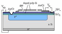
Development of photodetectors integrated with micromechanical and photonic components for MOEMS
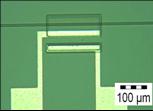
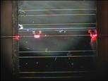
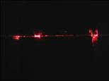
Tunable optical filter composed of a Fabry-Perot Interferometer (obtained by surface micromachining) integrated with a silicon photodiode.
Bilateral co-operation with LAAS CNRS Toulouse, France (Brâncusi project)
|
|
Tunable optical filter: a)structure; b)optical image |
************
WAFERBONDING AND ACTIVE PASSIVE INTEGRATION TECHNOLOGY AND IMPLEMENTATION (WAPITI)
STREP FP 6, Priority 2, IST
Coordinator - Fraunhofer Institute for Telecommunications, Heinrich Hertz-Institut, Berlin, Germany; Dr. Helmut Heidrich
Partners: National Kapodestrian Univ. of Athens (GREECE); Cambridge Univ., Engineering Depart.
(UNITED KINGDOM); EV Group, E. Thallner GmbH, Scharding (AUSTRIA); Max Planck Institute of Microstructure Physics, Halle (GERMANY);
National Institute for R&D in Microtechnologies, Bucharest (ROMANIA).
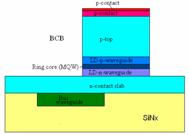
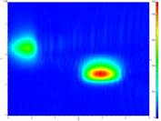
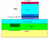
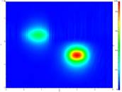
We calculated the bus-ring and the ring-bus coupling efficiency as a function of the lateral offset necessary for optimal working properties. Our theoretical and numerical results were confirmed by the experiments done upon the passive ring resonators realized by WAPITI consortium.
|
|
Vertically coupled micro-ring resonator -configuration I.
a) structure; b) radiation coupling from bus to ring |
|
|
Vertically coupled micro-ring resonator -configuration II: a) structure; b) Radiation coupling from bus to ring |
************
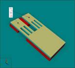
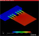
Movable micromirrors on silicon-on-insulator
Movable micromirrors are widely used in different types of applications such as miniature scanning devices, communication and sensors applications. These devices can be excited by different means, such as electromagnetic actuation, electrostatic actuation, piezoelectric actuation and thermal actuation.
Achievements: Design and simulation of movable micromirrors on silicon-on-insulator substrate thermally actuated based on bimorph layer (Au/SiO2 on Si). The response of the micromirrors, consisting in the displacement along z axe was investigated in static and dynamic regime using Coventor taking into account the material parameters and geometry of the structure.
MINASIST + project (2006-2008) contact person dr. Munizer Purica
|
|
Structure 3D |
Temperature distribution in the micromirror structure at 0,2 V |
|
|
Vertical displacement of the micromirror vs. applied |
Thermal transient response
for a period of 50 ms
|
5. Relevant equipments
Modeling and simulation tools:
- Opti FDTD 6.0 - design and simulation of advanced passive and nonlinear photonic devices
- Opti-HS - components and of active devices based on semiconductor heterostructures
- OptiBPM 8,0- design of complex optical waveguides, which perform guiding, coupling, switching, splitting, multiplexing and demultiplexing of optical signals in photonic devices
- OptiGrating- design software for modelling integrated and fiber optical devices that incorporate optical gratings
- LaserMod - analysis of optoelectronic devices by performing electrical and optical analysis of III-V and other semiconductor materials.
- Home made software based on C++ language for analysis of the reflection/transmission of the multiple layer systems. The software allows the analysis of 20 layers
- 3Lit – 3D micro-optical elements
- Coventorware
Technology (access)
- RIE, EBL, LPCVD, polymer technology
Characterization:
- spectrophotometers for UV-VIS-NIR and IR spectral range;
- spectroscopic ellipsometer
- AFM
- SEM.