¤ Results and News:
ISI papers
1. M. Aldrigo, D. Masotti, M. Dragoman, “Smart Two-Dimensional Material-based Time Modulated Array for RFID Applications,” IET Microwaves, Antennas & Propagation, vol. 11, no. 15, pp. 2267-2272, 2017 – corresponding author (ISI Journal), DOI: 10.1049/iet-map.2017.0309
2. M. Yasir,, M. Dragoman, A. Dinescu, M. Bozzi, S. Iordanescu, D. Vasilache, “Integration of antenna array and self-switching graphene diode for detection at 28 GHz,” IEEE Electron Device Lett., vol. 40, no. 4, pp. 628-631, Apr. 2019 – corresponding author (ISI Journal), DOI: 10.1109/LED.2019.2899028 (with acknowledgment to the project)
3. M. Dragoman, M. Aldrigo, J. Connolly, I. M. Povey, S. Iordanescu, A. Dinescu, D. Vasilache, M. Modreanu, “MoS2 radio: detecting radio-waves with a two-dimensional (2D) transition metal dichalcogenide semiconductor,” Nanotechnology 31 (2020) 06LT01, Nov. 2019 (ISI Journal), DOI: 10.1088/1361-6528/ab5123 (with acknowledgment to the project)
Conferences / Papers published in Proceedings
1. M. Aldrigo, M. Dragoman, D. Masotti, “Metal-Insulator Transition in Monolayer MoS2 for Tunable and Reconfigurable Devices”, Proc. of 41st International Semiconductor Conference (CAS), pp. 101-104, 10-12 October 2018 – “Best Paper Award CAS 2018”, DOI: 10.1109/SMICND.2018.8539834 (with acknowledgment to the project)
2. M. Aldrigo, M. Dragoman, S. Iordanescu, D. Vasilache, A. Dinescu, M. Shanawani, D. Masotti, “Graphene diodes for 5G energy harvesting: design, simulations and experiments,” Proc. of 49th European Microwave Week Conference, pp. 37-40, 29 September- 4 October 2019 (with acknowledgment to the project)
3. M. Aldrigo, M. Dragoman, S. Iordanescu, A. Dinescu, D. Vasilache, I. Povey, M. Modreanu, “Microwave detection with MoS2-based self-switching diodes,” accepted for oral presentation at the 42nd International Semiconductor Conference (CAS), 9-11 October 2019 (with acknowledgment to the project)
4. M. Aldrigo, M. Dragoman, S. Iordanescu, F. Nastase, D. Vasilache, and A. Ziaei, “Gain tunability of graphene patch antennas for the ISM band at 24 GHz,” iWAT2020 (2020 International Workshop on Antenna Technology), 25-28 February 2020, Bucharest, Romania, DOI: 10.1109/iWAT48004.2020.1570609136 – Invitated for an extended version to be published in “Sensors”, ISSN / eISSN: 1424-8220 (with acknowledgment to the project)
================
Results
================
Year 2018
First stage: Physical, chemical and electrical characterization of two-dimensional (2D) materials
Expected results:
- Investigation of physical, chemical and electrical properties of mono-atomic layers of molybdenum disulphide and other 2D materials grown via CVD (=chemical vapour deposition) method
- At least 1 paper in ISI journal and 1 paper presented at an international conference
Activity list:
- Activity 1.1: XRD, SEM and Raman analysis of mono- and multi-layer MoS2
- Activity 1.2: Design and simulation of test structures for electrical and high-frequency characterization of 2D materials
- Activity 1.3: DC and microwave/millimetre-wave characterization of MoS2-based test structures
- Activity 1.4: Dissemination of results
ACHIEVEMENTS:
During the first stage of the project, we have characterized two samples of mono-layer molybdenum disulphide (MoS2) on silicon dioxide/high-resistivity silicon (SiO2/HRSi) substrate, and one sample of mono-layer molybdenum disulphide on quartz, purchased from an international semiconductor company.
Raman, XRR (X-Ray Reflectivity) and GIXRD (Grazing Incidence X-Ray Diffraction) investigations demonstrated the mono-layer nature of MoS2 on SiO2/HRSi substrate, and the presence of a multi-layer MoS2 on quartz (at least 3 layers).
Problems of adherence of MoS2 on both substrates forced us to resume to a back-up solution: a partner which collaborates with IMT managed to fabricate via a combined ALD/CVD (ALD=Atomic Layer Deposition) process a 4-inch wafer of MoS2 multi-layer (15 layers) on Al2O3/HRSi. After a first basic material characterization, self-switching diodes (SSDs) were fabricated for DC characterization. Pictures are shown in Figs. 1a and 1b.
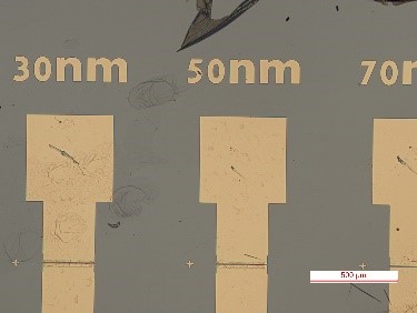
a. |
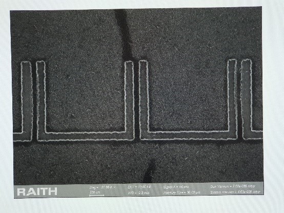 b. b.
|
| Fig. 1: Optical (a) and SEM (=Scanning Electron Microscope) (b) images of fabricated MoS2-based SSDs. |
This attempt was a technologic premiere in the realization of MoS2-based SSDs, since the current state-of-the-art relies for most only on simulations due to: (i) inhomogeneities in depositing a uniform MoS2 layer on a bulk substrate; (ii) presence of defects in the MoS2 layer; (iii) scarce adherence of the MoS2 layer to the bulk substrate.
The results of the DC characterization of the MoS2-based SSDs are shown in Figs. 2a and 2b.
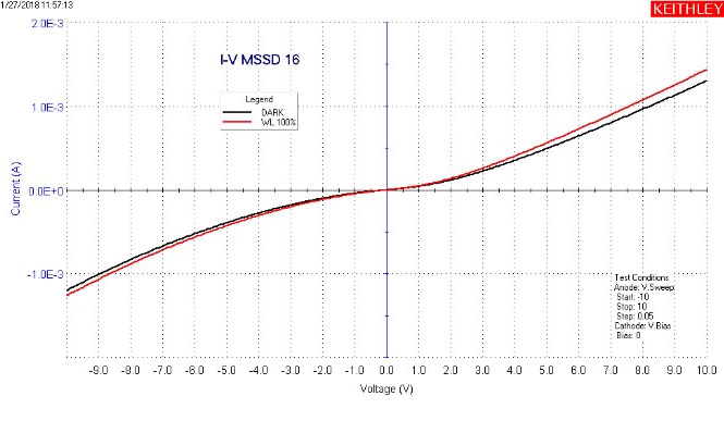
a.
|
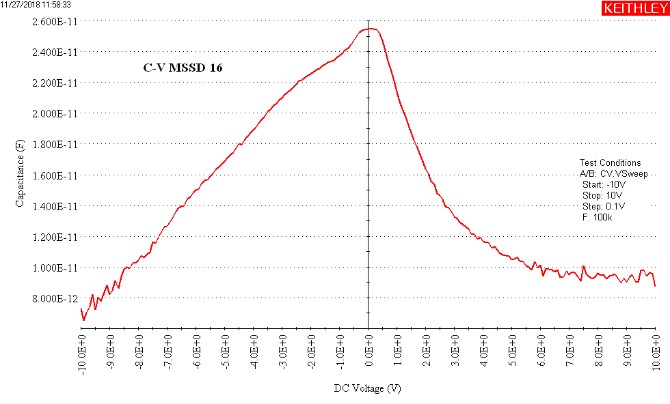
b.
|
| Fig. 2: Measured (a) I-V and (b) C-V curve of the fabricated MoS2-based SSDs. |
We have also achieved the following results:
- design of the high-frequency structures for microwave characterization of MoS2-based SSD;
- design and simulations of an X band (8-12 GHz) patch antenna based on MoS2 for a Time-Modulated Array (TMA) system, with reconfigurable properties thanks to the voltage-controllable physical properties of MoS2 (paper no. 2 in the list of published articles);
- design, simulation, fabrication and full DC/microwave characterization of a detector/energy harvester based on graphene SSDs, as benchmark case for MoS2-based SSDs (paper no. 3 in the list of published articles);
- contacted Thales company for a patent involving a MoS2-based reconfigurable antenna.
_________________________________________
Year 2019
Second stage: Electromagnetic (EM) and nonlinear design and fabrication of a Time-Modulated Array (TMA) system based on 2D materials for a “smart” RFID tag
Expected results:
- EM simulation of a single 2D material-based antenna with resonance frequency at microwaves or millimetre-waves
- EM simulation of array systems made of 2-4-8 antennas based on 2D materials
- Simulation of a 2D material-based switch
- Fabrication of a complete TMA system made of at least 2 antennas based on 2D materials
- At least 1 paper in ISI journal and 1 paper presented at an international conference
- Considering patenting the proposed system
Activity list:
- Activity 2.1: Electromagnetic simulation of a single antenna and of an array system made of 2-4-8 antennas
- Activity 2.2: Simulation of a 2D material-based switch
- Activity 2.3: Electromagnetic and circuit simulation of a complete TMA system
- Activity 2.4: Fabrication of a complete TMA system
- Activity 2.5: Dissemination of results
ACHIEVEMENTS:
During the second stage of the project, we have characterized in a complete way the 4-inch wafer of MoS2 on Al2O3/HRSi: Raman (Fig. 3) and TEM for thickness analysis, Spectroscopic Ellipsometry Mapping for confirmation of homogeneous deposition, Hall measurements for mobility, and 4-point probe measurements to determine MoS2 surface resistance.
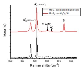 |
Fig. 3: Raman spectra of fabricated multi-layer MoS2 on Al2O3/HRSi. |
Thanks to the full characterization of the MoS2 wafer, we refined the design of the MoS2-based patch antenna in the X band. The antenna was simulated, fabricated and tested (Fig. 4), demonstrating tunable characteristics in terms of gain when applying to the MoS2 layer a DC bias voltage of some Volts.
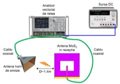 |
Fig. 4: Experimental set up for characterizing the MoS2-based patch antenna. |
These results have never been published before (and will be the object of a future paper for an ISI journal).
After that, we have designed, modelled, fabricated and tested MoS2-based SSDs working up to 10 GHz as both detectors and energy harvesters (Figs. 5a and 5b, papers no. 5 and 6 in the list of published articles). These results represent a technological premiere and have been published for the first time during this project.
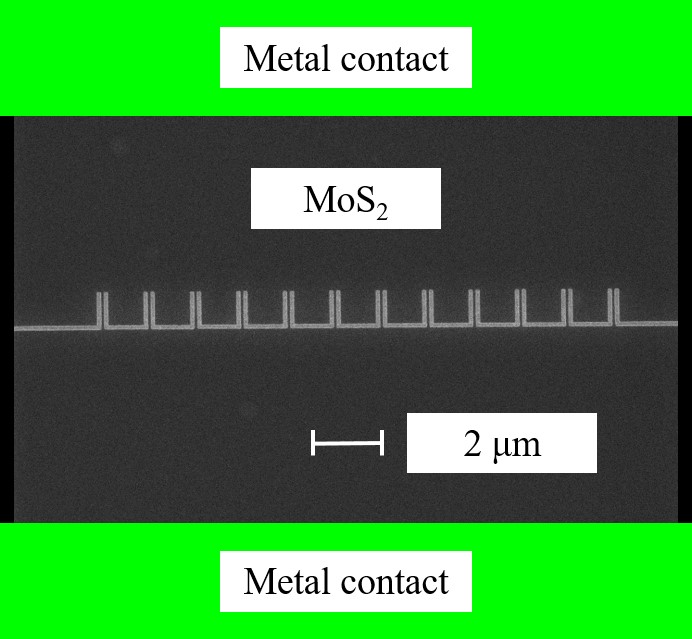
a.
|
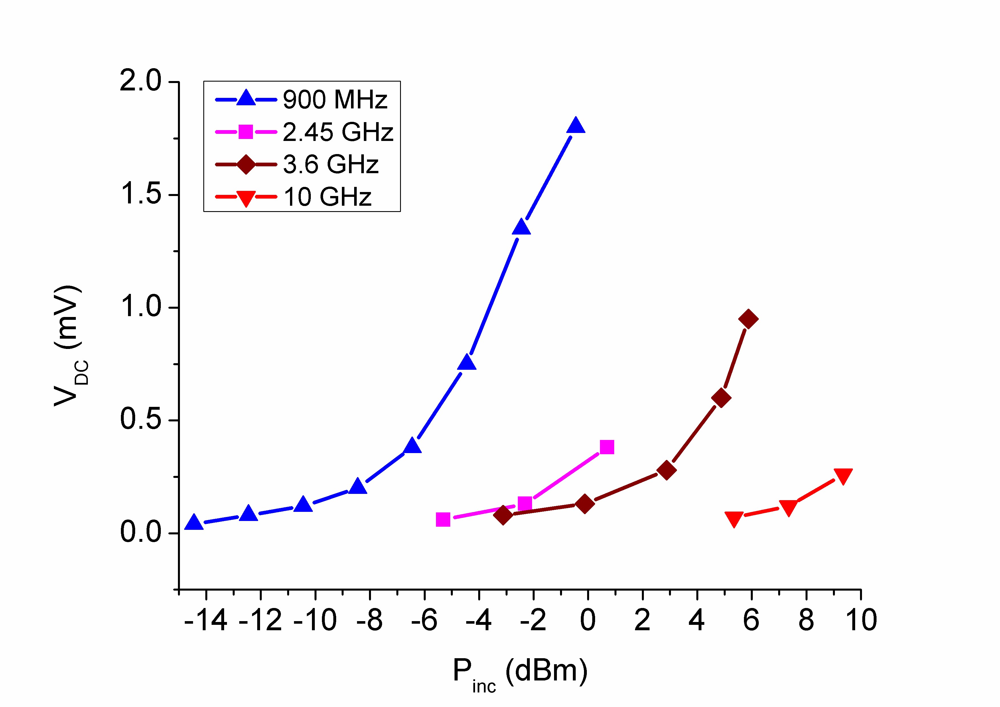
b. |
| Fig. 5: (a) SEM image of a MoS2-based SSD and (b) measured detected voltage at various frequencies. |
The next step was the simulation of two complete TMA systems (paper no. 1 in the list of published articles) made of two and eight MoS2-based patch antennas, using a 3D full-wave electromagnetic simulator and a customized nonlinear simulator. These results (very promising) constitute the base for the successive fabrication of a complete TMA system.
We have also achieved the following results:
- design, simulation, fabrication and full DC/microwave characterization of a 24 GHz MoS2-based patch antenna;
- preparation of a patent with Thales company for a MoS2-based reconfigurable antenna.
_________________________________________
Year 2020
Third (final) stage: Experimental characterization of a TMA prototype and its integration with a sensor
Expected results:
- Experimental characterization of the TMA system based on 2D materials in DC and at high frequencies
- Integration of the TMA system with a sensor and its characterization at microwaves
- At least 1 paper sent to an international conference
Activity list:
- Activity 2.1: Experimental characterization in DC and at microwaves/millimetre-waves of the TMA system
- Activity 2.2: Experimental characterization of the entire “smart” RFID system hybrid-integrated with a sensor
- Activity 2.3: Dissemination of results
ACHIEVEMENTS:
During the third (and last) stage of the project, we have fulfilled all the proposed targets of this project, paving the way to further promising research in this field.
First of all, we designed, fabricated and tested new SSD diodes based on MoS2/graphene heterojunctions in coplanar waveguide (CPW) technology (Fig. 6a). This type of diodes cannot be modelled with the Sichman-Hodges model, so that new strategies are being developed based on multiphysics simulations and the Foster method. In fact, in spite of its geometric nature, this heterojunction-based SSD diode works as a back-to-back diode at low voltage, and as a tunneling diode for a bias voltage higher than +10 V (Fig. 6b).

a) |
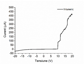
b) |
| Fig. 6: (a) Optical image of the fabricated heterojunction-based SSDs; (b) measured I-V characteristic. |
In Fig. 7, we show the signal detected by the heterojunction-based SSD diode at 2.49 GHz, which demonstrates how this device can be used as a detector (or even energy harvester) at microwaves.
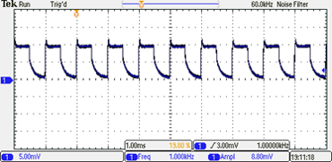
|
| Fig. 7: Detected signal at 2.49 GHz by the heterojunction-based SSD diode. |
Then, we re-designed completely the TMA system using graphene as 2D material. Thanks to its voltage-dependent conductivity, it is possible to fabricate tunable-gain antennas and TMA systems; hence, one can “smartly” transmit the desired amount of power by simply changing the bias voltage applied onto the graphene layer. The first promising results show a doubling of antenna gain when tuning monolayer graphene. These results are showed in Fig. 8 (G-CPA, paper no. 7 in the list of published articles).
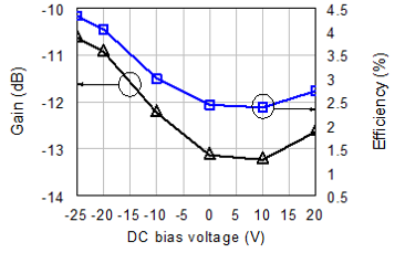
|
Fig. 8: Computed gain (solid black curve, left vertical axis) and radiation efficiency (solid blue curve, right vertical axis) of the proposed G-CPA, as a function of the applied DC bias voltage |
The results depicted in Fig. 8 led to the re-design of the final TMA system at 10 GHz, using graphene instead of MoS2. The final antennas/prototypes are shown in Fig. 9.
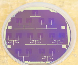
a) |

b) |
Fig. 9: (a) Optical picture of the fabricated graphene patch antennas, patch antenna arrays and TMA systems; (b) completed TMA systems for DC/RF characterization. |
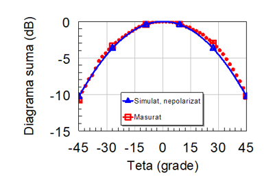
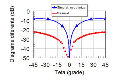
The characterization of the TMA system in Fig. 9b was aimed at measuring the “sum” and “difference” diagrams when piloting the two switches with a microcontroller through a precise time-dependent sequence of control pulses. The results of the combined electromagnetic/nonlinear simulations are in good agreement with the experiments (Figs. 10a and 10b).
a) |
b) |
Fig. 10: (a) Sum and (b) difference diagrams of the simulated (solid blue lines) and measured (dotted red lines) 2-antenna TMA system based on monolayer graphene. |
Finally, we tried to control the switches of the 2-antenna TMA system with a commercial SPE sensor for the determination of bisphenol A (BPA); more in detail, we tried to pilot the switches with the output voltage of the sensor. This way, we could “smartly” deploy the information in output from the sensor to send a tunable amount of power by using the proposed TMA system at 10 GHz. The hybrid integration of the TMA system with the sensor demonstrated the possibility of increasing the transmitted power up to 3 dB, hence realizing a “smart” RFID system for indoor localization.
Other results: we started the preparation of a patent with Thales company for a MoS2-based reconfigurable antenna.
_________________________________
¤ Project coordinated by:
National Institute for Reseatch and Development in Microtechnologies-
IMT Bucharest
http://www.imt.ro/ |
 |
|
|
¤ Project financed by:
|
|