
Welcome to dualSAW website!
Dual pressure and temperature sensors based on GaN membrane supported Surface Acoustic Wave (SAW) devices

Results
| 2022 | 2021 | 2020 |
| Rezultate (in Romanian) |
ESTIMATED RESULTS
- Fabrication of SAW devices on GaN membranes
- Characterization of the SAW structures
- Analysis of the behavior of the SAW sensors to simultaneous temperature and pressure measurements
- Dissemination of the results
OBTAINED RESULTS
Fabrication of the SAW sensors on GaN membranes
SAW structures with different IDTs width varying between 100 nm and 150 nm were fabricated on thin GaN membranes. Three types of membranes were etched: (i) GaN 0.7 μm thin; (ii) GaN/Si having 1.3 μm /10 μm thickness and (iii) GaN/Si/Mo 1.3 μm/ 10 μm/ 30 nm.
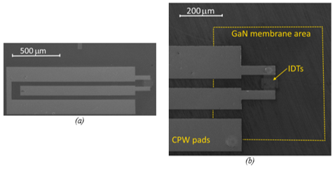
Figure 1 presents SEM images obtained with Scanning Electron Microscope - Vega II LMU (TESCAN), of a SAW structure having wIDT = 150 nm, fabricated on GaN membranes (membrane area of 500 μm x 500 μm).
 |
|
|
|
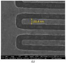
Figure 2 shows a SEM image of a GaN membrane intentionally broke for identifying its thickness and for evidencing the active area of the IDTs, suspended on the membrane
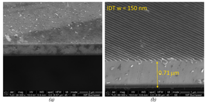 |
Fig. 2 SEM images with a detail of the broken GaN membrane (taken from the backside) (a) and on the frontside with the IDTs area (b) |
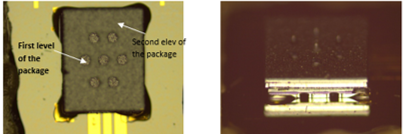
Packaging of the SAW sensors
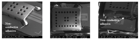
In the previous stage, different experiments were carried out to choose the proper materials for placing the capsules (different types of photoresists and non-conductive adhesives), the best results being obtained with a non-conductive epoxy type adhesive. The placement of the capsules in the center of the active IDTs area (Fig. 3) is done by a pick-and-place equipment, so a problem is the amount of the glue used - usually there is a surplus that can cover the side holes or affect the structures.
 |
|
Optical photos of the packaged structures are presented in Fig. 4
 |
|
Dual SAW sensor for pressure and temperature determination
The SAW structures were diced into chips and were hermetically soldered on a carrier, in order to keep constant the pressure underneath the membrane when external pressure is applied. The measurements were performed in a pressured chamber using Nitrogen atmosphere in the 0 to 12 Bars range. The temperature stability is an important criteria in the dual sensors behavior based on SAW resonators because the inevitable temperature variation due to gas compression or expansion caused by the variable nitrogen flow leads to the change of the resonance frequency of the sensors. The temperature in the pressured chamber should be carefully monitored along the measurements.
The reflection parameter S11 was measured with a vector network analyzer 37397D (Anritsu) and a pair of PM5 probes for on-wafer measurements from Suss Microtec. The first measurements were performed at room temperature and in atmospheric pressure.
The SAW structures having wIDT = 150 nm presented two resonant frequencies, identified as Rayleigh (R) and Lamb (L) propagation modes: fR = 7.17 GHz; fL = 12.9 GHz.
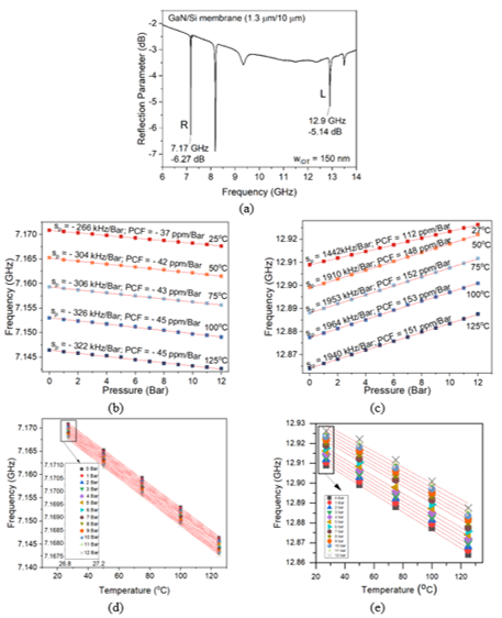 |
Fig.5 SAW structures on GaN/Si membrane, having wIDT = 150 nm: (a) reflection coefficient; pressure sensitivity determinations at different temperatures, Rayleigh mode (b) and for Lamb mode (c); temperature sensitivity determinations at different pressures for Rayleigh mode (d) and Lamb mode (e) |
For this type of structure, a linear variation of the resonance frequency with pressure and temperature was observed. The values of the pressure sensitivity (sP) and of the pressure coefficient in frequency (PCF) (at constant temperatures) were determined. The temperature sensitivity, sT varies between -401 kHz/°C and -450 kHz/°C and the temperature coefficient of frequency TCF varies between -31 ppm/°C and -35 ppm/°C, as function of the applied pressure. High values of the sensitivities sT and sP were obtained, very important for the resolution and the accuracy of the sensors.
Dissemination:
-
Publication of a research paper in IEEE Access – the simulation method described in the first 2 stages of the project was used for the SAW structures tested as temperature sensors:
George Boldeiu, George E. Ponchak, Alexandra Nicoloiu, Claudia Nastase, Ioana Zdru, Adrian Dinescu, Alexandru Müller, Investigation of Temperature Sensing Capabilities of GaN/SiC and GaN/Sapphire Surface Acoustic Wave Devices, IEEE Access, vol. 10, pp. 741-752, 2022, doi: 10.1109/ACCESS.2021.3137908. (Impact factor: 3.476)
-
Paper accepted for presentation at IEEE International Semiconductor Conference, 12 – 14 October 2022 – the results obtained for the packaged SAW sensor are presented:
D. Vasilache, A. Nicoloiu, G. Boldeiu, I. Zdru, A. Kostopoulos, M. Nedelcu, A. Stavrinidis, C. Nastase, G. Stavrinidis, G. Konstantinidis, A. Dinescu, A. Müller, Development of high frequency SAW devices devoted for pressure sensing, accepted la IEEE CAS 2022.
________________
ESTIMATED RESULTS
2nd stage:
- Simulations of the pressure and temperature behaviour for SAW devices supported on membranes and metalized membranes;
- Fabrication of the SAW devices supported on membranes and metalized membranes;
- Tests of the membrane supported SAW devices packaging;
- Characterization and analysis of the pressure sensitivity for the fabricated SAW devices;
- Dissemination of the results.
OBTAINED RESULTS
Simulations of the pressure and temperature behaviour for SAW devices supported on membranes and metalized membranes
The resonance frequency variation as function of the pressure (in the range of 1 – 7 Bar), for different temperatures (between 25 and 150oC), was extracted from coupled simulations (FEM+COM) for both propagation modes (Rayleigh and Lamb). This type of simulation is used for the first time for SAW structures supported on membranes. The variation of the resonance frequency versus pressure at different temperatures (Fig. 1), as well as versus temperature for different pressures (Fig. 2), can be linear approximated, confirming that this type of SAW structure can be used as dual sensor.
 |
 |
Fig. 1 The simulated resonance frequency vs. temperature, at different pressures for the SAW device supported on GaN membrane (1.3 μm thin) for Rayleigh propagation mode (a) Lamb propagation mode (b) |
Fabrication of the SAW devices supported on membranes and metalized membranes
First SAW structures having IDTs with digit/interdigit width of 100 nm and 120 nm have been manufactured on GaN membranes.
Three types of membranes have been etched: (i) 1.3 μm thin GaN membrane, (ii) 1.3 μm/10 μm thin GaN/Si membrane and (iii) 3 μm/10 μm/30 nm GaN/Si/Mo membrane.
The technological flow consists of 4 main steps: (1) the patterning of the CPW line – RF connection pads; (2) the fabrication of the interdigitated transducer (IDT) by nanolithography, the width of the digit/interdigit being 100 nm for one type of SAW structures and 120 nm for the second type; (3) supplementary metallization of the CPW line in order to ensure the thickness necessary for RF measurements and a good contact with the IDT area; (4) etching 500 x 500 µm area membranes under IDTs by dry etching (Reactive Ion Etching - RIE) of the silicon substrate.
SEM photos of SAW structures having IDTs with wIDT = 100 nm, supported on GaN/Si membrane are presented in Fig. 3.
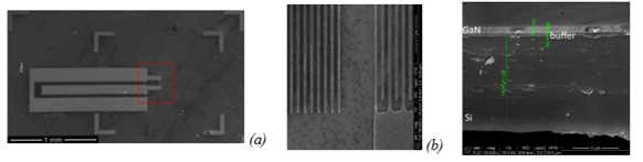 |
Fig. 3 SEM photos of SAW manufactured devices: (a) SAW device having 100 nm width of the IDTs, the membrane area is marked in red; (b) detail of the IDT and reflectors; (c) detail with the composition of the GaN/Si membrane |
Packaging of the SAW sensors
In order to ensure a minimum protection against the environment, a zero-level packaging was considered for the fabricated SAW structures, allowing in the same time the possibility to perform pressure and temperature measurements. The packages were fabricated by dry etching of Si wafers. SEM photos presents the junction between the package and the SAW structures through AZ 4500 photoresist (Fig. 4a) and epoxy adhesive (Fig. 4b).
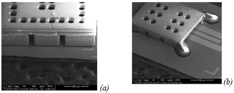 |
Fig. 4: SEM photos of packaged SAW structures sticked with: AZ 4500 photoresist (a) and epoxy adhesive (b) |
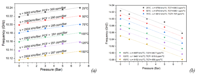
Pressure characterization
SAW structures have been diced into chips and then hermetically soldered on a metallic carrier (Fig. 5a) in order to obtain underneath the membrane a cavity, with quasi-constant pressure, that offers the possibility of deflection of the active area (with IDTs) on the membrane when an external pressure is applied. Initial, the reflection coefficient (S11) was measured at room temperature and ambient pressure with a vector network analyzer (VNA) type 37397D from Anritsu, with a PM5 on wafer set-up from Suss Microtec. Two resonance frequencies have been observed (f1 and f2 in Fig. 5b). The SAW devices have the resonance frequency > 10 GHz. The variation of the resonance frequency versus the applied pressure was measured in a pressure controlled chamber. The simulations have been validated by the pressure coefficient of frequency (PCF) obtained from measurements. The value of the PCF of 216 ppm/Bar, at room temperature, for Rayleigh mode is very close to the value of the PCF of 300 ppm/Bar obtained from simulations.
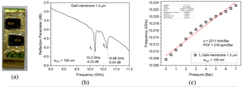 |
Fig.5 SAW structures (wIDT = 100 nm) supported on 1.3 μm GaN membrane soldered on a metallic carrier (a); Reflection parameter S11 (b); Resonance frequency f1 vs. pressure (c) |
Dissemination
A paper is in evaluation process at IEEE Access journal:
George Boldeiu, George E. Ponchak, Alexandra Nicoloiu, Claudia Nastase, Ioana Zdru, Adrian Dinescu, Alexandru Müller, Investigation of Temperature Sensing Capabilities of GaN/SiC and GaN/Sapphire Surface Acoustic Wave Devices, in review la IEEE Access.
________________
ISI papers:
1. Alexandra Nicoloiu, George E. Stan, Claudia Nastase, George Boldeiu, Cristina Besleaga, Adrian Dinescu, Alexandru Müller, "The behaviour of gold metallized AlN/Si and AlN/glass based SAW structures as temperature sensors," in IEEE Transactions On Ultrasonics, Ferroelectrics, And Frequency Control, vol. 68, no. 5, May 2021, DOI: 10.1109/TUFFC.2020.3037789
ESTIMATED RESULTS
1st stage: Simulation of membrane suspended SAW structures (August-December 2020)
- Electromechanical simulation of SAW structures suspended on GaN and GaN/Si membranes
-
The coupled FEM+COM simulation of membrane supported SAW structures at room temperature and atmospheric pressure
-
The coupled FEM+COM simulation of backside metallized membrane supported SAW structures at room temperature and atmospheric pressure
-
Webpage implementation
RESULTS OBTAINED
Electromechanical simulation of the backside metallized GaN membrane supported SAW structures
 |
 |
Fig.1 The mode shape for Rayleigh resonance frequency for the SAW structure on GaN (1.3 μm) membrane, having 50 nm Au on the backside, wIDT=150 nm; (a) Anti-symmetric Rayleigh mode f+ = 5.049 GHz; (b) Symmetric Rayleigh mode f- = 6.52 GHz |
|
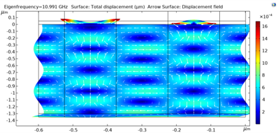 |
Fig.2 The symmetric Lamb mode shape (10.99 GHz) for the SAW structure on GaN (1.3 μm) membrane, having 50 nm Au on the backside; IDTs w=150 nm; hAu=50 nm |
The coupled FEM+COM simulation of backside metallized membrane supported SAW structures at room temperature and atmospheric pressure
A new simulation method was implemented for extracting an optimum admittance for the SAW structures realized on GaN and GaN/Si membranes. The method couples FEM (Finite Element Method, COMSOL) with „Coupling of Modes” and it was presented the first time for the temperature SAW sensors realized on AlN/Si and AlN/Glass in the published paper: A. Nicoloiu, et. al, IEEE Transactions On Ultrasonics, Ferroelectrics, And Frequency Control, vol. 68, no. 5, May 2021. The advantage of this method resides in taking into account the reflectivity and the attenuation. In the frame of dualSAW project this method is adapted for the dual pressure and temperature SAW sensors on thin GaN membranes.
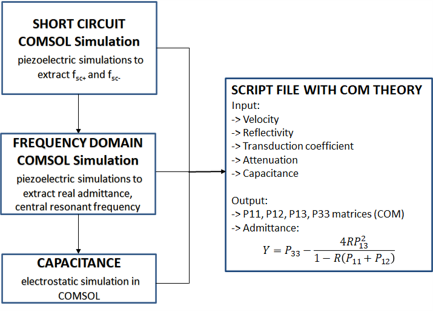 |
Fig.3 The symmetric Lamb mode shape (10.99 GHz) for the SAW structure on GaN (1.3 μm) membrane, having 50 nm Au on the backside; IDTs w=150 nm; hAu=50 nm |
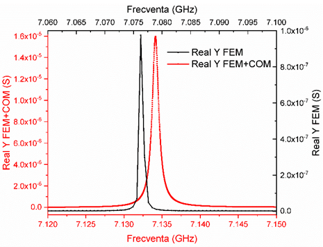
A comparison between the admittance extracted from the FEM (COMSOL) and the coupled simulation are shown below for the three envisaged structures. An improvement of three orders of magnitude in the amplitude of the admittance was obtained by including COM in the simulation procedure.
 |
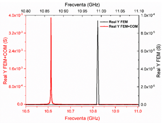 |
Fig.4 Real part of the admittance extracted from the coupled FEM – COM simulation (red) compared to the FEM simulation (black) for the backside metallized GaN membrane supported SAW structure C: (a) Rayleigh mode; (b) Lamb mode. |
|