

| MINAFAB | Characterization equipments |
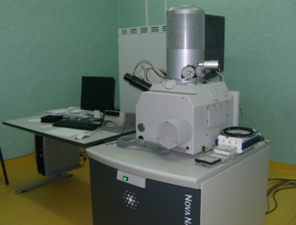
Nova™ NanoSEM 630
Technical characteristics: The FEI Nova NanoSEM 630 is a high-quality nanoscale research tools for a variety of applications that involve sample characterization, analysis, prototyping, and S/TEM sample preparation. It features a superior low voltage resolution and high surface sensitivity imaging in the range of Ultra high Resolution Field Emission Scanning Electron Microscopes (UhR FE-SEM). The Nova NanoSEM 630 presents also low-vacuum imaging capabilities for spectacular nanoscale characterization on charging and/or contaminating nanotech materials. The Nova NanoSEM 630 also offers the most extensive set of tools for nanoprototyping, including an on-board digital pattern generator and dedicated patterning software, a high speed electrostatic beam blanker, gas injection systems for direct electron beam writing of nanostructures and its high stability 150 mm piezo stage.
|
|
Basic hardware features:
|
||
Applications: |
||
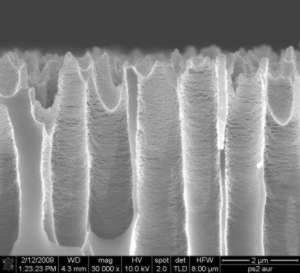
On a variety of challenging nanotechnology materials such as metals, magnetic materials, nano-particles and powders, nano-tubes and -wires, porous materials (e.g. silicon), plastic Electronics, glass substrates, organic materials, diamond films, cross-sections etc
|
||
|
Results:
|
|
|
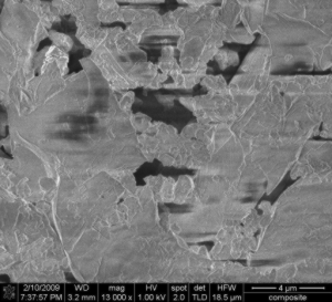
Detail of MRS 4.1-calibration standard used in nanometrology. |
|
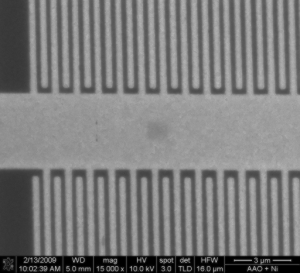
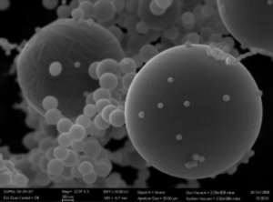
Micro and nanospheres produced in the process of CNTs growth. |
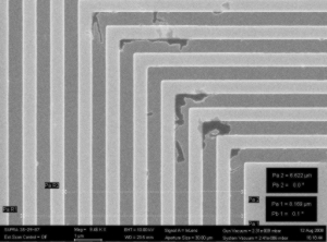
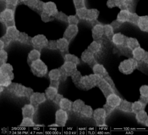
Porous silicon covered with gold nanoparticles by sputtering. |
|
****************************************************************** |
||
Partneship: CATHERINE- Carbon nAnotube Technology for High-speed nExt-geneRation nano-InterconNEcts, STREP, FP7-ICT, 2008-2011 |
||
|
||
Application scientist: Phys. Adrian Dinescu, adrian.dinescu@imt.ro |
||
|
|
Last update: March 5, 2012 |