| Types of services provided by IMT-MINAFAB |How IMT-MINAFAB is operating? |
IMT policy related to MINAFAB |Description of the main equipments | How to access IMT-MINAFAB? |
| Interested in cooperation with IMT? |
Description of the main equipments
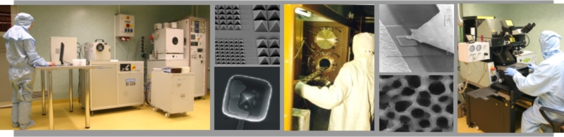
The main equipments available through IMT-MINAFAB are listed here. For some entries, apart from the description of the equipment, you may find a range of applications and specific results.
Main Capabilities
Main Tools
Process Capabilities
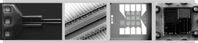
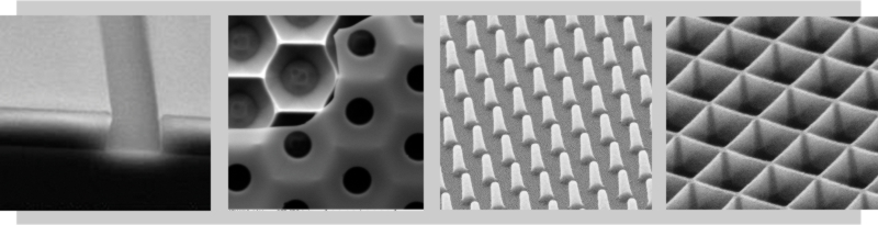
Lithography for MEMS, Bio-MEMS, MOEMS, RF-MEMS
- Proximity/contact/flood exposure: 365nm (1000 W, Hg), 249nm (500 W, Hg/Xe)
- Single/double face alignment
- Laser exposure lithography: 0.6µm
- Mask copy, photo-repeating
- Development
- Precision e-beam lithography
- Mix-and-match lithography
- E-beam nanoengineering
- Induced nanodeposition (Pt, W, SiO2)
- Induced etching (C, SiO2)
Direct micro/nanodeposition of spots and patterns (molecules, precursors, nanodots)
- Microarray spot plotting and scanning
- Programmable dip-pen nanopattern printing
Physical depositions (10-7 mbar; Al, Ni, Cr, Au, Pt, Ti, W, AlSi etc.)
- E-beam evaporation
- DC-sputtering
- Thermal
Dry Etching (CF4, SF6; O2, Ar; 13,56MHz, 600W)
- RIE silicon,
- RIE polysilicon
- RIE oxide
- RIE nitride
Wet/electrochemical etching
Thermal Processes (4")
- Dry oxidation
- Wet oxidation
- Annealing
- RTP, RTA, RTO
- Deposition from liquid source POCl3
- Deposition from solid source BN, B+, P+
- Solid state diffusion
- Nitridation, Silicidation
- Crystallization, Densification
- Alignment/sintering processes(forming gas)
Chemical depositions (under development)
- PECVD - Silicon oxide
- PECVD - BPSG
- PECVD - Silicon nitride
- LPCVD - Polysilicon
- LPCVD - Low stress silicon nitride
- LPCVD - Silicon oxide
Rapid Prototyping
- 3D printing (under development)
- Laser microstructuring (under development)
- Micromold fabrication
Beam characterization
- SEM
- Field-emission SEM
- X-ray: HRXRD, WAXRD (with/without focalisation, with and/or without monochromation, with and/or without analyzer crystal), SAXS, XRR, XRPD, GIXRD, IGPID
Scanning Probe characterization
- AFM -dry
- AFM - wet cell
- STM
- NSOM
- SECM
Device characterization and reliability testing
- Electrical probing I/V (DC...65GHz)
- Simple and/or combined device stresses - humidity, temperature, pressure, vibration, mechanical shocks
- MEMS defect analysis, accelerated testing
Spectroscopic characterization (thin films, nanomaterials)
- Spectroscopic ellipsometry
- HR-Raman
- Fluorescence
- EIS
- UV-Vis-NIR
- FTIR
Other inspection
- Confocal optical microscopy
- Optical profilometry
Surface chemistry and wafer cleaning
Porosification by electrochemical anodisation
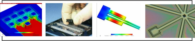
Wafer dicing, die bonding, wire bonding
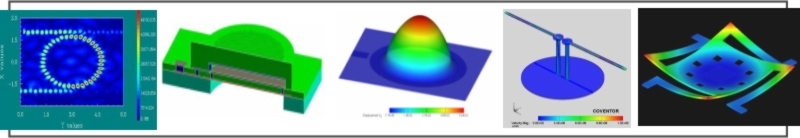
CAD and Simulation Capabilities
(Coupled) field analysis for MEMS (static, transient, harmonic)
- Electrostatic and electroquasistatic
- Mechanical
- Thermomechanical
- Piezoelectric
- Electromechanical
- Electrothermomechanical
- Piezoresistance
- Piezoelectric
- Squeeze-film or free-space fluid damping
- Proof mass or plate inertia
Design and simulation of microfluidic components and systems
- Flow in microchannels, micromixers, microfilters - flow under pressure drop; thermal flow; fluid mixing; thermal analysis; electrokinetic with field switching; droplet and bubble simulation (fomation, transport, merging/splitting, interaction to walls); component separation from mixtures; fluid-structure interaction phenomena
- Micropumps and microvalves with various actuation principles - electrostatic, piezoelectric, pneumatic, electroosmotic
- Multi-species chemical reaction analysis
CAD and simulation for passive/active micro-photonic components
- Photonic crystals
- Ring resonators
- Optical wave guides
- Optical integrated circuits (active and passive)
- Diffractive micro-optical elements
CAD and dimulation of RF-MEMS components and circuits
Models for ready-to-manufacture devices
Constructive optimizations
Mask design and simulation of technological processes
Geometrical modeling (e.g., AFM image reconstruction in CAD format, generation of analytically defined surfaces)
Statistics for experimental data
Data analysis and visualizations
Training in CoventorWare, ANSYS, Opti FDTD, IE3D, etc.
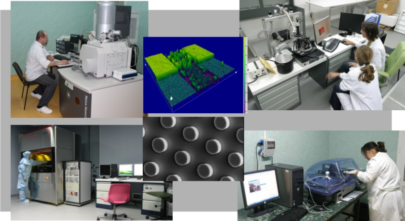
Main Technological and Characterization Tools
Microlithography tools
- Laser lithography system - DWL 66 fs, direct writing laser, high resolution pattern generator (Heidelberg Instruments Mikrotechnik, Germany); [details]
- Double Side Mask Aligner - MA6/BA6 (Suss MicroTec, Germany); [details]
- Wafer spinners - DELTA 10 (Suss MicroTec, Germany), etc. [details]
- Wafer Bonder System- SB6L- Wafer - Substrate Bonder System [details]
Physical deposition tools
- Electron Beam Evaporation - TEMESCAL FC-2000 (Temescal, USA), metalic thin laers deposition for transfering the mask geometris on substrate followed by lift-off. [details]
- Electron Beam Evaporation an DC sputtering system - AUTO 500 (BOC Edwards, UK); [details]
- Electron Beam Evaporation equipment Elettrorava ER-EB12 (Elettrorava, Italy); [details]
Chemical deposition tools
Dry etching tools
- RIE Plasma Etcher - Etchlab 200 (SENTECH Instruments, Germany); [details]
- DRIE- Plasmalab System 100- ICP Deep Reactive Ion Etching System [details]
Thermal processing tools
- Furnace - oxidation, diffusion, sintering - Lindberg [details]
- Furnace - rapid thermal processing/annealing - AS-One (AnnealSys, France) - [details]
SEM; Electron-beam lithography; Nanoprinting
- Electron beam lithography and nanoengineering workstation - e_Line (Raith, Germany ) [details]
- Field Emission Gun Scanning Electron Microscope (FEG-SEM) - Nova NanoSEM 630 (FEI Company, USA) [details]
- Scanning Electron Microscope - Vega II LMU @ Pattern Generator - PG Elphy Plus (TESCAN s.r.o , Czech Republic @ Raith, Germany) [details]
- Dip Pen Nanolithography Writer - NSCRIPTOR (NanoInk, Inc., USA) [details]
SPM: AFM, STM, LFM, Phase Imaging, Force Modulation, Force Spectroscopy, SNOM, confocal, SECM
- Scanning Probe Microscope - NTEGRA Aura (NT-MDT Co., Russia) [details]
- Scanning Near-field Optical Microscope - Witec alpha 300S (Witec, Germany) [details]
- Scanning Electrochemical Microscope - ElProScan (HEKA, Germany) [details]
Nanomechanical characterization tools
- Nanomechanical Characterization equipment - Nano Indenter G200 - (Agilent Technologies, USA) [details]
Diffractometry; Interferometry; Spectroscopy; Voltammetry
- X-ray Diffraction System (triple axis rotating anode) - SmartLab - 9kW rotating anode, in-plane arm (Rigaku Corporation, Japan) [details]
- High Resolution Raman Spectrometer - LabRAM HR 800 (HORIBA Jobin Yvon, Japan) [details]
- Spectroscopic ellipsometer - SE 800 XUV (SENTECH Instruments, Germany) [details]
- White Light Interferometer - Photomap 3D (FOGALE nanotech, France) [details]
- Combined Time Resolved and Steady State Fluorescence Spectrometer - FLS920P (Edinburgh Instruments, UK) [details]
- FT-IR spectrometer, with FT-Raman module - VERTEX 80/80v with RAM II FT-Raman Module / Bruker Optics /2015 [details]
- Electrochemical Impedance Spectrometer - PARSTAT 2273 (Princeton Applied Research, USA) [details]
- Voltammetry and polarography analysis system - TRACELAB 50 (Radiometer Analytical, France)
- Dynamic Electrochemical Laboratory - VoltaLab 40: PGZ301 Universal Potentiostat/ Galvanostat & VoltaMaster 4 software (EIS, Voltammetry) (Radiometer Analytical, France)
- UV-VIS-NIR Spectrophotometer - SPECORD M42 (Zeiss, Germany) [details]
- Fourier–Transform Infrared Spectrometer - Tensor 27 (Bruker Optics, Germany) [details]
- UV-Vis-NIR Thermo-Electric Cooled Fiber Optic Spectrometer - AvaSpec-2048 TEC (Avantes, The Netherlands) [details]
- NIR Spectrometer - AvaSpec NIR256-2.2 (Avantes, The Netherlands) [details]
- Refractometer for layer thickness measurements - NanoCalc-XR [details]
Microarrays, Biomolecule research
- Micro-Nano Plotter - OmniGrid ( Genomic Solutions Ltd., UK) [details]
- Microarray Scanner - GeneTAC UC4 (Genomic Solutions Ltd., UK) [details]
- Zeta Potential and Submicron Particle Size Analyzer - DelsaNano (Beckman Coulter, USA) [details]
Probers, on-wafer; electrical characterization
- Microwave network analyzer (0.04-65 GHz) with Manual Probing Station - Lightning 37397D VNA/Anritsu; PM5/Suss MicroTec (Anritsu, Japan; Suss MicroTec, Germany) [details]
- Wafer Probing Station - Easyprobe EP4 (Suss MicroTec, Germany) [details]
- Semiconductor Characterization System (DC) with Wafer Probing Station - 4200-SCS/C/Keithley Easyprobe EP6/ Suss MicroTec (Keithley Instruments, USA; Suss MicroTec, Germany) [details]
- Semiconductor Characterization System - 4200-SCS, C-V 3532-50, DMM 2700-7700, 2002, 6211-2182 (Keithley Instruments, USA) [details]
Reliability and Testing Tools
- Climatic Chamber - CH 160 (Angelantoni, Italy) [details]
- Thermal shock chamber - TSE-11-A (Espec Europe, Germany) [details]
- Free Fall Shock Machine - 0707-20 (MRAD, USA) [details]
- Highly Accelerated Stress Test Chamber - temperature, humidity, pressure, polarization - EHS-211M (Espec Europe, Germany) [details]
- Mobile Thermal Airstream System - ThermoStream TP04300A-8C3-11 (Temptronic, USA) [details]
- Electrodynamic vibration system with thermal and electrical tests - TV 55240/LS (TIRA, Germany) [details]
- Universal Ovens with electrical testing - UFB (Memmert, Germany) N6711A (N6741B,N6743B,N6746B,N6773A) (Agilent Tehchnologies, USA)[details]
Wetbenches
- Masks processes: resist development, Cr etching, resist removal, DI cleaning; Acid processes and DI rinsing; Solvent bench; (Atechim, Romania) [details]
- Other wet processes (Salare, USA)
Other tools
Computation, Simulation and Design Tools
Coupled analysis for MEMS
- CoventorWare 2008.010 (COVENTOR, USA)
- Modules: ARCHITECT, DESIGNER, ANALYZER, MemElectro, MemMech, CoSolveEM, MemETherm, MemPZR, MemPZE, Damping MM, InertiaMM, MemHenry, MemCFD, Netflow, SwitchSim, ReactSim, MemFSI, BubbleSim, DropSim, SEMulator3D, EM3D
- Ansys Multiphysics 11.0 (ANSYS, USA) - Structural, thermal, acoustic, electromagnetic and coupled field analyses, CFD
Photonic components: simulation, modeling and design
- Opti FDTD 8.1, Opti-HS, OptiBPM 9.0, OptiGrating (Optiwave, Canada)
Microwave and millimeter wave circuits and microsystems: design and modeling
- IE3D, FIDELITY (Zeland, USA)
Other tools
- TransMagic STANDARD (TWeatherford, USA)
- SolidWorks Office Professional (SolidWorks, USA)- 3D CAD design software
- Mathematica 7 (Wolfram, USA)
- Matlab 7 (The MathWorks, USA)
- Modules: Simulink, Curve Fitting Toolbox, Extended Symbolic Math, Genetic Alghoritms, Image Processing, Neural Network, Optimization Toolbox, Signal Processing, Spline Toolbox, Statistic Toolbox
- OriginPro 8 (OriginLab, USA) - data analysis and graphing workspace, analysis tools for statistics, 3D fitting, image processing and signal processing
- COMSOL Multiphysics 3.3 and 3.4 (enabling parallel computation)
- Visual Studio 2008 Pro Programming tool for RAD and IDE.
top
________________________________________________________________________