Description
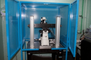
The HEKA ElProScan is an Electrochemical Probe Scanner for various investigations of electrochemical active surfaces. It belongs to the family of the scanning microscopes like AFM, STM or SECM. The system exists of three main units, a positioning system, a Bipotentiostat/Galvanostat and a data acquisition system.
System components
• Positioning system with 3 stepper motors and a piezo translator mounted on a granite portal including fundamental plate
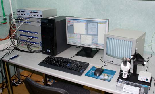
• Bipotentiostat/Galvanostat PG 340 with two low current Preamplifiers (see also data sheet "PG 340 Bipotentiostat/Galvanostat" and "Low Current Preamplifier")
• Software POTPULSE with SCAN extension (see also data sheet "POTPULSE")
• Real-Time Computer System with real-time processing boards, counter and data acquisition modules.
EIProScan features:
- The HEKA ElProScan is the only system which can perform measurements in an extremely wide current range up to 2 A. It also operates as a standard (Bi-) potentiostat/Galvanostat, thus, making it usable for many other electrochemical applications also.
- Low current preamplifiers allow high-resolution low-noise recordings in the low pA range.
- High precision real time controlled positioning system mounted on a stable holder made of granite, resolution in XY: 100 nm or 15 nm stepper motors, resolution in Z: 100 nm stepper motor + Fast real time controlled Z-piezo with 5 nm resolution and 100 mm scan range, closed loop regulated.
- The system comprises a large scan area (50 mm on each axis) with accurate position control and a fine piezo-driven z positioning.
- With electrodes in the sub micrometer range, the Faradaic current at the tip of the electrode becomes very small, making high demands on the amplifier.
- The smallest resolution for a scan step is 15 nm and 100 nm for the high resolution and standard stepper motors, respectively. The scan speed ranges from 15 nm/s (high resolution motors) to 100 mm/s.
|
|
|
Applications:
Imaging and positioning
A three-dimensional SECM image is obtained by scanning the tip in the x-y plane and monitoring the tip. A particular advantage of SECM in imaging applications, compared to other types of scanning probe microscopy, is that the response observed can be interpreted based on fairly rigorous theory, and hence the measured current can be employed to estimate the tip-substrate distance. Moreover, SECM can be used to image the surfaces of different types of substrates, both conductors and insulators, immersed in solutions. The resolution attainable with SECM depends upon the tip radius. For example, local activity of an enzymatic reaction on a filtration membrane can be determined
Studies of heterogeneous electron transfer reactions
SECM can be employed in heterogeneous kinetic studies on various metal, carbon and semiconductor substrates. For example, the measurement of the very fast kinetics of the oxidation of ferrocene at a Pt UME has been carried out. The technique can also be applied to measure kinetics of reactions at the interface between two immiscible solutions (for example, water/oil). To perform a measurement, one records the tip-current as the tip is approached toward the interface. The experimental tip-current versus tip-substrate distance curve is then matched with computer simulated curves and the value of the speed of reaction occurring at the interface can be obtained.
Studies of homogeneous chemical reactions
The TG/SC (with small tip and substrate) mode of SECM, in the same manner as the rotating ring disk electrode (RRDE), is particularly suitable for the studies of homogeneous chemical kinetics. The SECM approach has the advantage that different substrates can be examined easily, i.e., without the need to construct rather difficult to fabricate RRDEs, and higher interelectrode fluxes are available without the need to rotate the electrode or otherwise cause convection in the solution. Moreover, in the TG/SC mode, the collection efficiency in the absence of perturbing homogeneous chemical reaction is near 100%, compared to significantly lower values in practical RRDEs. Finally, although transient SECM measurements are possible, most applications have involved steady-state currents, which are easier to measure and are not perturbed by factors like double-layer charging and also allow for signal averaging.
Characterization of thin films and membranes
SECM is also a useful technique for studying thin films on interfaces. Both mediated and direct electrochemical measurements in thin films or membranes can be carried out. For example, polyelectrolytes, electronically conductive polymers, passivation films on metals and dissolution processes have been investigated by SECM. Membrane transport: the transport of chemicals through natural or artificial membranes, and biological tissues. SECM seems to be particularly suited for such studies because in many cases the transport happens through micro pores in the material and therefore is spatially constricted. Elucidating transport mechanisms can help understand the functionalities of biological tissue such as skin, dentine, or cartilage.
Liquid-liquid interfaces
One of the most promising applications of SECM is the study of charge transport at the interface between two immiscible electrolyte solution (ITIES). Charge transfer processes across the ITIES with or without membranes can be studied.
Probing patterned biological systems
SECM can be used to probe artificially or naturally patterned biological systems. Both amperometric and potentiometric techniques with ion-selective tips can be used.
Fabrication
The SECM can be used to fabricate microstructures on surfaces by deposition of metal or other solids or by etching of the substrate. Two different approaches could be used, the direct mode and the feedback mode. Typically, in the direct mode, the tip, held in close proximity to the substrate, acts as a working electrode (in deposition reactions) or as the counterelectrode (in etching processes). The feedback mode of fabrication utilizes the same arrangement as in SECM imaging. The tip reaction is selected to generate a species that reacts at the substrate to promote the desired reaction, i.e., deposition or etching.
****************************************************************** |