

| MINAFAB | Characterization equipments |
Semiconductor Characterization System with Manual Probe Station
Technical characteristics: Model-4200 SCS/C/Keithley, EP6/ Suss MicroTec Description The equipment performs electrical measurements for a wide range of applications from materials research and nanostructures development to I-V characterization of nanoelectronic devices. Semiconductor Characterization System 4200-SCS configured with the 4200-PA Remote Preamplifiers, offers exceptional low current measurement capability with a resolution of 0.1 fA and 5 mV. The software of the system is a Keithley Interactive Test Environment (KITE) for device characterization application. It provides advanced test definition, parameter analysis and graphing. KITE contains several projects. Each project is dedicated for a specific set of measurements. Default project includes standard tests for MOSFETs, BIPOLAR transistors, resistors, and diodes. Other projects are: MEMORY projects, CMOS project, NANOTECHNOLOGY project that include tests for nanowires, nanotubes, molecular CNT transistors and biocomponents. ********************** |
|
Applications:
**************************************************************************************** |
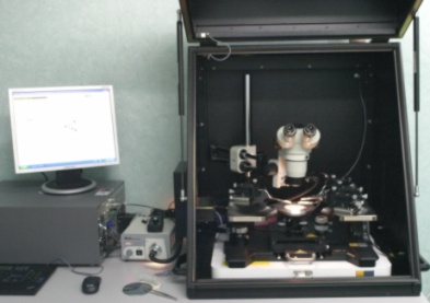 |
Results: The equipment has been aquired in the frame of the Project 11-048/2007-2010, Electronic Nanodevices Based on Oxidic Materials- NANOXI, research project coordinated by IMT, funding from national programme PNCDI2. The equipment is used to perform electrical characterization of MOSFET nano-demonstrators which use ultrathin oxidic films doped with Rare Earth ions (MOx RE) or Transition Metal ions (MOx TM). The measurements capabilities of the tool will provide a better understanding of the fundamental phenomena of conduction and fotodetection in electronic nanodevices based on oxidic materials, as well as characterization of advanced electronic devices capable of using the quantum properties associated with the electron spin.*****************************************************************
|
Application scientist: |
|
|
Last update: March 06, 2012 |