Scanning Probe Microscope NTEGRA Aura - NT-MDT
Technical characteristics:
Scanning Probe Microscope (SPM) performs 3 dimensional imaging of the topography and studying other physical properties of sample surfaces on a scale from microns down to the nanometric level.
Measurements could be done in ambient atmosphere or in controlled atmosphere.
- Scan range: 100x100x10 μm.
- Non-linearity in X, Y with closed-loop sensors < 0.15 %.
- Positioning sensitivity: 2 μm
|
|
Description:
The equipment enables several related techniques for high resolution imaging and measuring of surfaces, the properties which could be characterized depending on the chosen technique.
Main applications - in the field of surface metrology, for quantitative measurements of the 3D surface topography for a large variety of samples.
Key advantages of the technique as compared with other microscopies as optical and SEM :
- ability of measuring the vertical dimensions of the samples together with lateral ones with little or no sample preparation required
- samples could be measured in various environments (normal ambient, controlled gaseous, liquid, low vacuum)
The range of samples that could be imaged: very large, no matter of the sample conductivity, covering metallic, ceramic, polymeric and semiconducting materials .
Briefly: The SPM microscope could in principle image and perform three dimensional measurements of any surface features from surface roughness to nanometer-sized features.
********************** |
Application fields:
- Evaluation and optimization of thin film coatings for various applications (optical, packaging, paintings, wear-resistant etc);
- High-resolution surface profilometry;
- Grain and particle size analysis;
- Surface cleaning and polishing studies (Characterization of optical surfaces roughness, electro-polished metal surface evaluation etc);
- Microstructural studies (Pharmaceutical, Polymers);
- Morphological studies of biological and biocompatible materials;
- Virtually any other field where nanometer-sized surfaces are concrened;
********************** |
Examples of provided services:
- Surface morphology inspection;
- Quantitative measurement of surface features at nanometric level;
- Nano-surface texture/ roughness measurement;
|
| Results: |
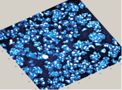
AFM image of a ZnO thin film on Si. Scan range: 40x40 microns.
The AFM image was used for evaluating the growth pattern of ZnO, for applications in optolectronic devices and gas sensors.
|
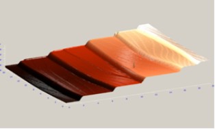
AFM image of step patterned Si. Individual step height: 15 nm. Individual atomic planes could be noticed in the 3D rendered image.
|
|
Partneship:
******************************************************************
|
| Application scientist: phys. Raluca Gavrila, [email protected] |
|
HOME |
 |
Last update: March 5, 2012 |
|