|
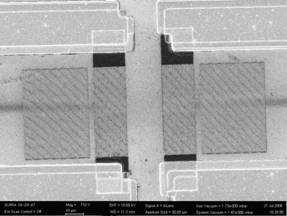
SEM image of a SAW test structure having digits with 250n width |
|
Details of the SAW test structure having digits with 250n width |
|
a b |
|
c d |
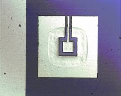
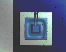
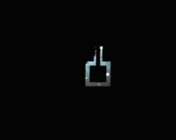
FBAR structures micromachined on thin GaN membrane: (a), (b) top view of structures having thick MoAu electrodes, (c) top view of structure having Mo electrodes, (d) bottom view with top illumination for the (c) structure
|
|
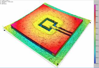
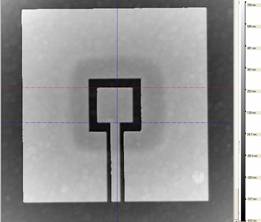
White light interferometry 3D analysis for a FBAR structure on GaN membrane |
|
White light interferometry 2D analysis for a FBAR structure on GaN membrane |
|
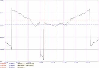
White light interferometry analysis for a FBAR structure on
GaN membrane-the profile along the feeding line |
SAW resonator manufactured on AlN/Si with 5 GHz resonance frequency
|
SAW structured were manufactured on AlN layer grown on high resistivity silicon having the resonance frequency around 5 GHz. The resonators have two identical interdigitated transducers (IDT) structures and two reflectors. The IDTs have digists and interdigits with 300nm width (spacial periodicity is λ = 1.2 µm), procesed by nanolithografic techniques. |
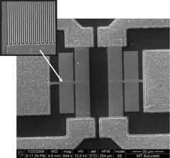
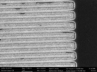
SEM image of a SAW structure manufactured on AlN
|
| |
Microwave characterization |
|
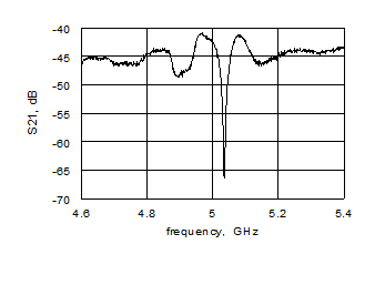 Transmision measurements –S11 versus frequency
 |
|
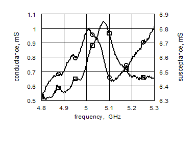
Input conductance measured for an IDT (left axe, curve with squares) and the measured susceptance (right axe ; curve with circles) obtained from the measurements from S11
|
SAW resonators manufactured on GaN/Si for frequences higher than 5 GHz
|
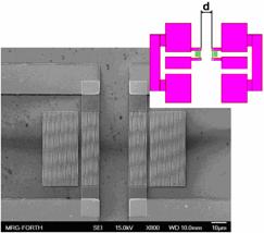
Using nanolithografic techniques, SAW structures having IDTs with 30 digits having digists and interdigits with 200nm width and 50 µm legth. The IDT structures are face to face at four different distances d= 20µm, 100 µm, 200 µm and 600 µm. |
|
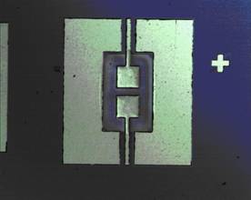
SEM image of a SAW structure manufactured on GaN/Si; the full structure in the inset |
Microwave characterization
|
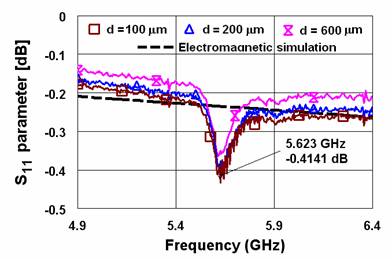
Measured reflection losses (S11) versus the frequency for three structures with different distances between the IDTs compared with the electromagnetic simulated results (without the inclusion of the piezoelectric effect).
|
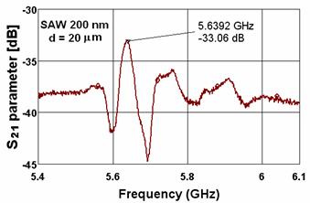 Transmission measurements for the SAW test structure having a 20-µm distance between the IDTs
 |
 Transmission measurements for the SAW test structure having a 1000-µm distance between the IDTs.
|
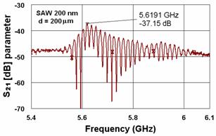
Transmission measurements for the SAW test structure having a 200-µm distance between the IDTs.
|
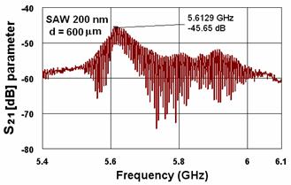
Transmission measurements for the SAW test structure having a 600-µm distance between the IDTs.
|