RESULTS OBTAINED IN 2015
1. Preliminary tests for sinterization and characterization of aluminium nitride films sintetised by reactive magnetron sputtering and multiparameter characterisation
The achievement of a good crystallinity degree, as well as a high c-axis texturing, is conditioned by the base pressure attained in the reactor chamber prior to the admittance of the high purity working gases (Fig. 1-a,b). Moreover, in this second project stage, it was evidenced that the c-axis orientation of the AlN films is improving with the deposition time (and consequently the increase of the film thickness), such that at a film thickness of ~3 µm, one can obtain a full-width at half maximum of the (002) rocking curve <4°, which falls within the project goals
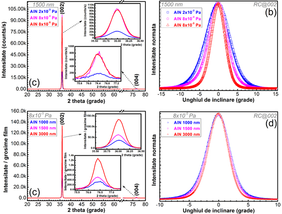 |
(a,c) XRD patterns recorded in θ – θ symmetric geometry and (b,d) the rocking curves corresponding to the AlN (002) reflexions. (a,b)Structural quality dependence of the base pressure, in the case of AlN films with thickness of 1500 nm deposited onto Si (100) wafers by reactive magnetron sputtering at low temperature (~50°C). (c,d) Crystallinity and c-axis texturing dependence on films thickness, in the case of AlN samples synthesized onto Si (100) wafers by reactive magnetron sputtering at low temperature (~50°C), starting from a base pressure of 8x10⁻⁵ Pa. |
In the case of AlN films prepared using the optimized deposition conditions, the dielectric constant was found to be around 12. The conductivity value depends on the AlN film thickness, and consequently of their structural quality. For AlN films with thicknesses of 600 and 1300 nm, were obtained conductivity values of ~4.5 x 10⁻¹⁰ S and ~3 x10⁻⁹ S, respectively.
2. Design and modelling of SAW structures for temperature senzor with IDTs having submicronic dimensions
2D modelling and simulations with the finit elements method (using COMSOL programme) for a SAW resonator (on AlN piezoelectric material) have been performed. The device will be a temperature sensor, therefore the model will include the temperature dependence.
The modelling has the following 5 steps:
1. Conceptual modelling: elaborating the ipothesis and the neglected elements
2. mathematical modelling: the elaboration of the model in mathematical language
3. Elaborating the equations for the input and out put elements
4. numerical modelling elaborating an algorithm for the model equations solutions
5. Validate and check the model: the elaborated model is validate using the simulation results afther implementing thenuerical algorithm in the system computation
3. Technological manufacturing of SAW test structures
In this stage masks have been manufactured in order to obtain SAW resonators with various configurations of the interdigitated transducer (IDT) : width/space digit/interdigit of 200 nm, 170 nm and 150 nm, therefore the obtained resonance frequency is in the range 7.64 GHz - 10.06 GHz. All IDTs structures have 150 digits and 150 interdigits of length 100µm and 50µm; at each side of the interdigitated structure there is a pair of 50 reflectors at different distances. IDTs metallization was performed using electron beam nanolithography (EDL) to obtain IDTs metallization of 100nm Ti/Au (5nm/95nm) thickness.
4. Microphisical and microwave characterisation of SAW structures for temperature sensing.
SAW structure has been designed for working frequencies> 8GHz: IDTs have 200-150nm obtained by nanolothographi process.
|
|
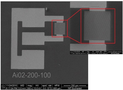
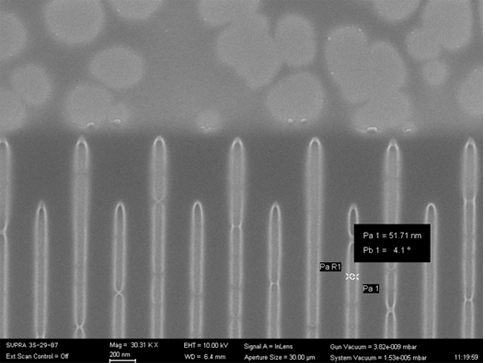
SEM image of SAW structure |
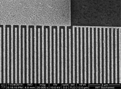
Detail of the SAW structure with digits and interdigits of 200nm width-SEM image |
SAW on AlN/Si structures have been characterised in microwave using an Anritsu Vector Network Analyzer in association with an Microtec prober (measurements on wafer).
|
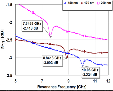
Resonance frequencies at room temp (T = 23 ºC) for SAW strctures with IDT of 200nm(pink curve, ) 170 nm (red curve) si 150 nm (blue curve) |
5. Temperature dependence of experimental structures for temperature sensors (including measurements in cryostat for low temperatures)
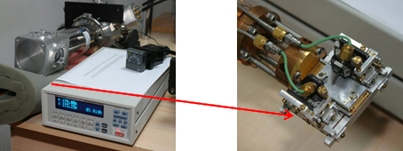
Temperature characterization of SAW structures have been performed in the -140ºC - 150ºC range, using the cryostat (model SHI-4H-1, Janis Research Company). That equipment has high precision and a large temperature scale. The SAW structures have CPW conecting pads for the indoor manufactured measuring system inside the cryostat.
|
|
Janis Cryostat equipment |
Special support for temperature measurements inside the cryostat |
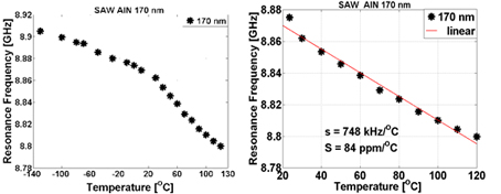
We present the curve for the resonance frequency variation with the temperature in the 20-120ºC range. From the slope of this almost linear curve, we have obtained the SAW resonator temperature sensitivity of S=84 ppm/ºC.
|
Resonance frequency with temperature in the rang -140, 130 ºC for SAW structure with digits width 170nm (a); SAW resonator temperature sensitivity (b) |
RESULTS OBTAINED IN 2014
Preliminary synthesis experiments of highly c-axis textured aluminum nitride thin films by reactive magnetron sputtering. Multiparametrical characterization
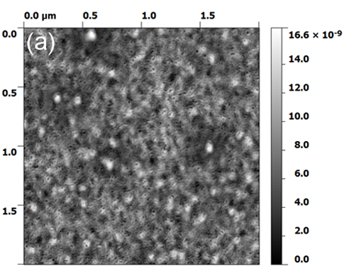
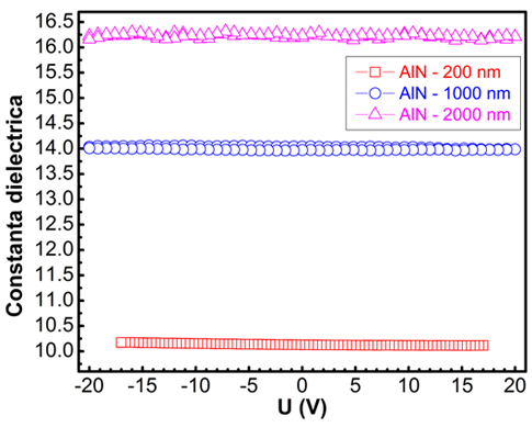
Preliminary synthesis experiments of AlN thin films having various thicknesses (~200 nm, 1000 nm and 2000 nm) have been carried out onto high resistivity silicon (100) wafers by reactive radio-frequency magnetron sputtering (RF-MS). We aimed to evaluate insightfully their optical, morphological, structural and electrical properties (spectroscopic elipsometry, X-ray diffraction, Fourier transform infra-red spectrometry, atomic force microscopy, and measuring the dielectric constant and electrical losses) in order to identify the necessary strategies to be applied in the future stages of the project, capable to lead to the improvement of the physico-chemical quality of AlN films, and thereby, to the maximization of the functional response of the sensor devices. The RF-MS deposition process was performed at a total gas pressure of 0.2 Pa in a argon-nitrogen mix atmosphere (nitrogen volumetric concentration: 30%), at room temperature (in this case the substrate reached a maximum temperature of ~50oC, attributed solely to the plasma bombardment) and on heated substrate at 750oC (intending to survey the possibility of enhancing the crystalline status of the deposited films). The gas flow has been maintained in all cases at a constant value of 40 sccm. The physico-chemical analyses performed in the framework of the 1st Project stage have indicated that the successful synthesis by RF-MS of highly c-axis textured hexagonal aluminum nitride thin films (FWHM of the rocking curve~4.6o), exhibiting low surface roughness (~1.2 nm), a high dielectric constant (~14-16) and reduced electrical losses, occurred at a low substrate temperature (~50oC). In the next project stage the research team will attempt to enhance the degree of c-axis texturing of AlN films by tailoring the RF-MS variables.
 |
 |
 |
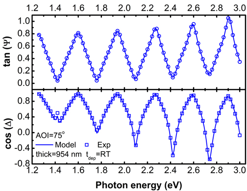
Ellipsometry spectra of the AlN film synthesized at room-temperature (thickness ≈954nm). |
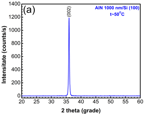
Typical XRD diagram recorded in symmetric geometry (θ–θ) for AlN films synthesized at room-temperature |
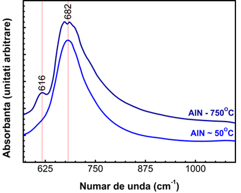
Comparative FTIR spectra of AlN films deposited at low (~50oC) and high (750oC) temperature |
 |
 |
Typical AFM image of a AlN film surface deposited at room-temperature |
Dielectric constant vs. Voltage dependence of AlN films having thicknesses of ~200 nm, 1000 nm and 2000 nm |
Nanolithography tests for WBG semiconductors; test metallization processes for IDTs with nanometric fingers and interdigit spacing
The nanolithographic tests have studied the main parameters for obtaining desired geometry : (i) beam size (the degree of focus); (ii) writhing speed; (iii) acceleration voltage; (iv) current of the beam
 |
 |
 |
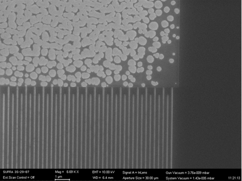
“Under-exposed ”SAW test structure |
Details of the “under-exposed structure |
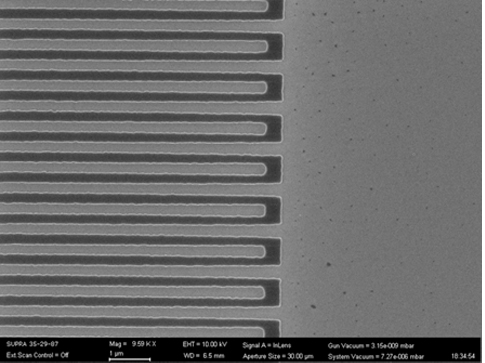
SAW structure processed after optimization of the nanolithography parameters |
Metallization tests have analyzed the problems that can occur when exposure of the photoresist is not enough to complete removal of the areas we wish to configure or when the metallization layer is too thick and problems during lift-off process appears. These issues have been solved and SAW structures with the desired metallization layer have been processed.
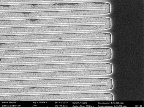 |
Details of the SAW test structure having a good metallization |
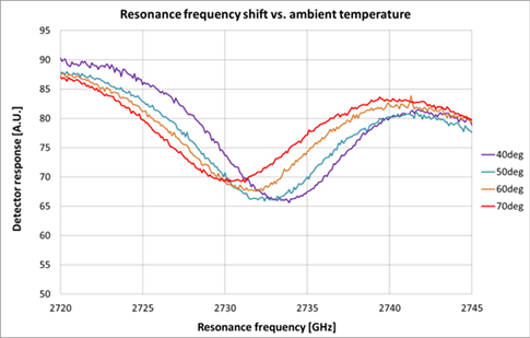
Preliminary tests for accurate reading of the resonant frequency (with wire)
Measurements were made at four levels in the ambient temperature, the results were obtained by placing the sensor in a thermo-stated chamber (oven); the graphs have shown a good precision, but with the option to be further improved.
 |
Results of the preliminary tests |