RESULTS OBTAINED IN 2016
1. Sinterization and characterization of highly textured c-axis AlN thin films
In the third stage of the project were identified the optimized parameters (i.e., base pressure: ~4 x 10⁻⁵ Pa, total working pressure 0.2 Pa, partial nitrogen pressure 0.05 Pa) for the fabrication of a thin AlN film, with thickness of ~1 μm, having a full width half-maximum of the 002 rocking curve lower than 4° (Fig. 1a). The morphological, structural, compositional and mechanical characteristics of this type of layer were investigated using a plethora of advanced analysis techniques (SEM, AFM, TEM, XRD, SAED, EDS, XPS, pull-out tests, nano-indentation assays, nano-scratch tests, and nano-wear measurements). The XPS analysis revealed a concentration of Al-O-N bonds of ~5% (which indicates the low oxygen contamination of the AlN film) (Fig. 1b), whilst the TEM investigations evidenced the compact and uniform morphology of the optimized AlN film (Fig. 1c,d). This type of AlN film elicits an excellent bonding strength to the Si substrate (~47.6±2.6), and possesses an elastic modulus close to bulk AlN values (342.3±16.9 GPa), hardness higher than the bulk AlN (26.4±0.8 GPa), and very good resistance to scratch and wear tests (wear rate at 6 mN: 8.6*10-7 mm3/Nm).
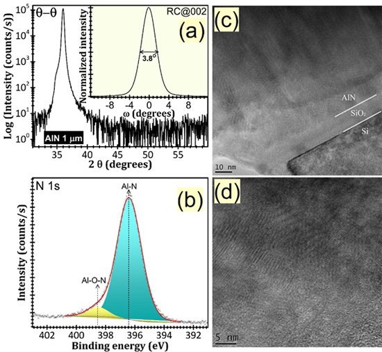 |
(a) Typical XRD diagram recorded in θ–θ symmetric geometry and the corresponding 002 rocking curve of the optimized AlN thin film. (b) N 1s core level XPS spectrum of the AlN film. Symbols represents the experimental data, the curves indicate the overall fit and identified components. (c,d) Cross-sectional TEM images of AlN thin film: general morphology (c); high-resolution micrograph (d). |
2. Modelling of SAW structures for temperature sensor
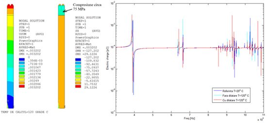
The modeling task of this year addressed the effect of the temperature. Two aspects were considered:
1) the dependence with respect to the temperature of material properties, namely the Young modulus, for an equivalent isotropic piezoelectric material and
2) the thermal expansion both by means of the strains that depend on the coefficient of the thermal expansion and the considering of a prestress in the model, due to the initial thermal expansion that induces mechanical stress in the model due do different expansion coefficients of the substrate and the piezoelectric.
The numerical results show that indeed, the increase of the temperature leads to a frequency shift with sensitivity of the order of hundreds of kHz/degrees C and a TCF of tens of ppm/degrees C.
|
|
Distribution of the total displacements [um] and stresses [Mpa] obtained from a static thermal simulation. The latter are used as a prestress for frequency domain analysis. |
Frequency characteristic of the electric charge of the terminal in three cases: reference (20 degrees C), with modeling of the temperature dependence of the Young modulus (120 degrees C), with the consideration of the thermal expansion. |
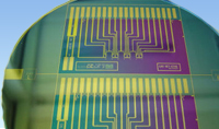
3. Technological manufacturing of the demonstrator
The technological process starts with patterning the pads that connects the nanometric IDTs. Lift-off process is used and the TiAu metallization has a total of 220 nm (20 nm/200 nm). IDTs metallization was performed using electron beam nanolithography (EDL) to obtain IDTs metallization of 100nm Ti/Au (5nm/95nm) thickness. 200nm width PMMA resist was used. The process follows with the metallization of the IDTs, also by lift-off.
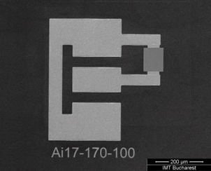 |
SEM image of the SAW structure |
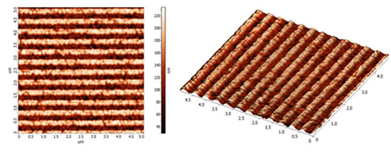
4. Microphysical and temperature characterization of the optimized structures for the temperature sensor based on SAW resonators on AlN
|
AFM characterization of the SAW/AlN structures |
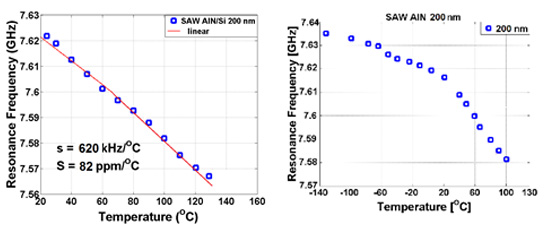
From the microwave measurements, performed on wafer using the existing equipment (VNA), the S11 parameter was used, in order to have information regarding the dependence of the resonance frequency vs. temperature and to determinate the sensitivity.
|
|
Variatia frecventei de rezonanta cu temperatura a rezonatorului SAW |
Sensibilitatea cu temperature structura sensor SAW in intervalul 20-120ºC |
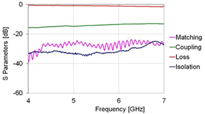
5. Preliminary tests for accurate wired reading of the resonant frequency
For the accurate wired reading system, a wide band directional coupler with multiple sections, was manufactured. The couplig factor has a slow and monotonous variation between 4GHz and 7 GHz and an isolation coefficient greater than 25 dB up to 7 GHz.
|
The characteristics of the directional coupler measured in the 4=7 GHz range |