
Welcome to SiC-MOS website!
Advanced processing for stability improvement in SiC-MOS devices
Results
| Stage 2, December 2021 | Stage 1, December 2020 |
In Romanian
Rezultatele obținute prezentate succint:
Rezultatul semnificativ al proiectului constă în obținerea unor capacitoare MOS fabricate pe SiC, stabile pe o gamă largă de temperaturi și la aplicarea unor câmpuri electrice mari pe electrodul de poartă.
Performanțele acestor dispozitive constau în:
- reducerea densității de sarcină efectivă din oxid
- scăderea densității stărilor de lângă interfața oxid/SiC
-
creșterea tensiunii de străpungere
- scăderea curenților reziduali (de pierderi).
Toate aceste rezultate au fost obținute prin dezvoltarea unor etape tehnologice care au constat în: oxidări termice in mediu uscat (O2) a plachetelor de SiC, depuneri de oxizi (cu constantă dielectrică mare) prin tehnica ALD (Atomic Layer Deposition), dezvoltarea unor tratamente termice post-oxidare în atmosferă de B, respectiv POCl3.
_____________________
SiC MOS capacitors based high k dielectrics were fabricated in order to allow a better exploitation of the SiC properties by reducing the field strength within the dielectric and diffusion of metals, improving the overall reliability of the gate oxide. A common applicative issue for high k dielectrics on SiC is represented by the high leakage currents attributed to a lower theoretical band offset value (ΔEC = 1.5 - 1.7 eV), in comparison with the SiO2/4H-SiC system (ΔEC = 2.7 eV).
Five batches of SiC MOS capacitors were fabricated, as is illustrated in Fig. 1.
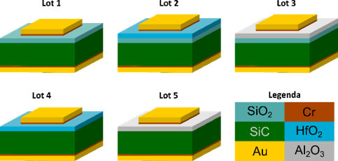 |
Fig. 1 Designed of the SiC MOS capacitors |
Lot 1: As oxidized SiC MOS capacitor. The MOS oxide was grown at a temperature of 1100℃, time for 30 minutes, in dry oxygen atmosphere;
Lot 2: 6 nm of HfO2 was deposited by using Atomic Layer Deposition technique on the grown SiO2 film;
Lot 3: 6 nm of Al2O3 was deposited by using Atomic Layer Deposition technique on the grown SiO2 film;
Lot 4: 6 nm of HfO2 was deposited directly on SiC by using Atomic Layer Deposition technique;
Lot 5: 6 nm of Al2O3 was deposited directly on SiC by using Atomic Layer Deposition technique.
The fabricated SiC MOS capacitors were microphysical (X-Ray Reflectivity - XRR) and electrical (capacitance-voltage (C-V) and current-voltage (I-V) measurements) characterized in order to identify and diminish the main sources of the device instability.
The XRR measurements confirms the desired thickness of the high k dielectrics, as it is illustrated in Fig. 2.
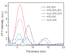 |
Fig. 2 The experimental Fast Fourier Transform spectra for the fabricated samples |
In Fig. 2 we can observe the thickness of each oxide film, identified by the peak. In the case of the samples with stack oxides (SiO2 and high k dielectrics), we can identify two peaks. The first one represents the SiO2 thickness and the second is the sum of the two oxides.
The electrical measurements were performed in order to determine both the effective oxide charge (C-V characteristics) and barrier height between SiC and oxides conduction bands (I-V characteristics). In Fig 3 are presented both C-V (experimental and ideal curves) and I-V curves.
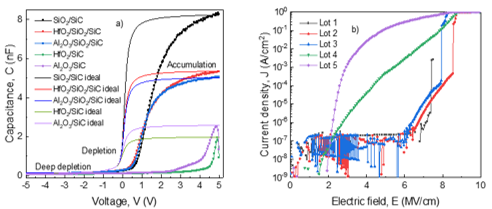 |
Fig. 3 a) C-V and b) I-V characteristics for the fabricated SiC MOS capacitors |
Using the characteristics from Fig. 3a, the effective oxide charge density (Qeff) was determined based on the difference between the experimental and ideal C-V curves. A value of 8.22 x 1012 cm-2 was obtained for the SiC MOS capacitor from the batch no. 1 (Lot 1). This value was diminished with the high k dielectric thin films deposited on the grown SiO2 film, reaching values of 4 x 1012 cm-2 for Lot 2 and 3.75 x 1012 cm-2 for Lot 3. Higher values for Qeff were obtained for the SiC MOS capacitors from Lot 4 and Lot 5, but still smaller than the one reported in Lot 1.
In Fig. 3b, there are presented two distinct conduction mechanisms in the fabricated SiC MOS samples: a Fowler-Nordheim (F-N) mechanism (for the Lot 1, Lot 2 and Lot 3) and a thermionic emission one for the samples from Lot 4 and Lot 5. Using the F-N formalism, the barrier height between SiC and oxides conduction bands was calculated. A value of 3.7 eV was obtained for the sample from Lot 1 and values more appropriate from the ideal one (2.7 eV) were determined for the samples fabricated in Lot 2 (2.44 eV) and Lot 3 (2.34 eV). Moreover, the SiC MOS capacitors from Lot 2 and 3 show higher breakdown electric fields in comparison with the capacitor from the Lot 1.
In conclusion, high k dielectrics can improve seriously the stability and reliability of the SiC MOS devices.
______________________
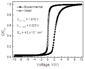
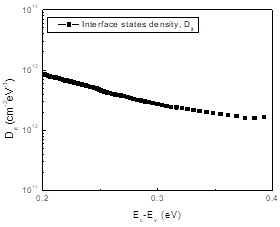
SiC MOS capacitors were fabricated in order to evaluate both the electrical defects from the oxide/SiC interface and the oxide charges from the thermally grown oxide. Two circular active areas were designed in order to be further tested as a differential gas sensor. The effective oxide charge was determined based on the deviation of experimental C-V curves from ideal ones, leading to a value of 4.2 x 1012 cm-2. The interface states’ density was calculated based on the Terman method, demonstrating a decrease from near the SiC conduction band (8.5 x 1012 cm−2 eV−1) to deeper inside the gap (1.6 x 1012 cm−2 eV−1).
The fabricated samples were packaged in compact TO-39 capsules using wire-bonding technology and electrical tested using a Keithley 4200 semiconductor characterization system, at room temperature and dark conditions.
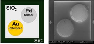 |
| Fig. 1 Designed structures and SEM image of the SiC MOS capacitors’ active areas |
In order to obtain information about the oxide/SiC interface properties, C-V measurements at high frequency (1MHz) have been performed on the test structures.
 |
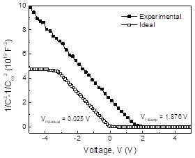 |
| Fig. 2 Experimental and ideal C-V curves for the fabricated SiC MOS capacitor | Fig. 3 1/C2 vs. applied voltage. |
After a linear fitting process performed on both these curves (in the -2 V – 0 V range), the resulting slope and intercept values were used to determine flat band voltages, which are also given in Fig. 3.
The Dit distribution in the SiC band gap was determined. The corresponding values are plotted in Fig. 4, as a function of energy levels in the SiC band gap, between 0.2 and 0.4 eV.
 |
| Fig. 4. Dit distribution in SiC band gap |
Fig. 4 emphasizes that Dit values decrease from near the conduction band (0.2 eV), where a value of 8.5 x 1012 cm−2 eV−1 is reported, to deeper inside the gap (0.4 eV), where a plateau value of 1.6 x 1012 cm−2 eV−1 is reached.
Diseminare:
1 articol: R. Pascu, „Ultrashallow defects in SiC MOS capacitors”, Solid State Electronics Letters, Vol. 2, 2020, pp. 79-84. ISSN 2589-2088. https://doi.org/10.1016/j.ssel.2020.11.001