Main results obtained in 2013
Dielectric and metallic layer depositions were optimized for higher quality and better control over the deposited thickness/uniformity. Fig. 1 shows a SEM (Scanning Electron Microscopy) image of a 1250 nm thick gold layer. The metal layer was obtained through sputtering of Cr/Au (20/200 nm), followed by electrochemical deposition of 1000 nm of gold. The silicon dioxide layers were obtained through thermal oxidation (about 1500 nm thick), while the low stress silicon nitride layers were obtained through LPCVD (Low Pressure Chemical Vapor Deposition), with a deposited layer thickness of about 600 nm.
The plasma etching process was optimized, using the Bosch process in a ICP-RIE (Inductively Coupled Plasma – Reactive Ion Etching). For etching mask definition, the following sequence was optimized: HPR 504 lithography (1200 nm thick photoresist), silicon nitride etching through the photoresist mask with RIE and wet etching of SiO2 through the same photoresist mask, in a Buffer solution.
The electromagnetic modeling and design results obtained during the previous year were used to design and fabricate masks for test structures. Fig. 2 shows the mask set. There were several fabrication runs, with the goal of technologic flow optimization and improvement of fabrication yield. In order to reduce the costs, low resistivity silicon wafers were used, which affect the performances of some millimeter wave structures.
Antenna test structures, supported by thin dielectric membranes were fabricated and are under test (Fig. 3).
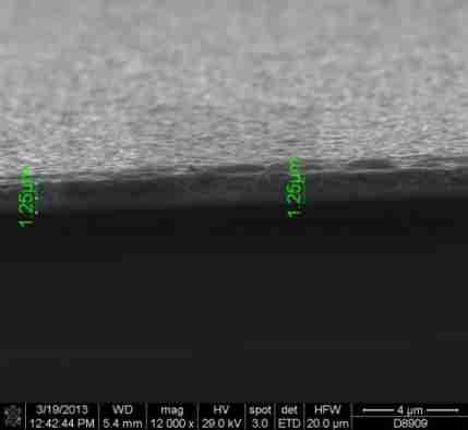
Fig. 1 SEM photo of the gold layer (~1250 nm thick)
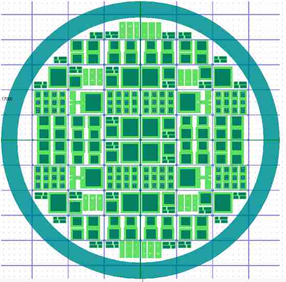
Fig. 2 Mask set used for the test structure fabrication
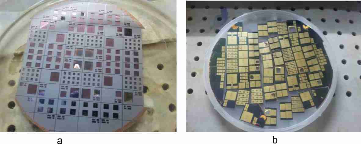
Fig. 3. Test structures fabricated in 2013: (a) back side view; (b) front side view