Project results
I. Publications in ISI journals
- J. Tomaschko, S. Scharinger, V. Leca, J. Nagel, M. Kemmler, T. Selistrovski, S. Diebold, J. Jochum, R. Kleiner, and D. Koelle, Phase-sensitive evidence for dx2-y2 pairing symmetry in the parent-structure high-Tc cuprate superconductor Sr1-xLaxCuO2, Physical Review B 86, 094509 (2012) [download paper]
- J. Tomaschko, V. Leca, T. Selistrovski, S. Diebold, J. Jochum, R. Kleiner, and D. Koelle, Properties of the electron-doped infinite-layer superconductor Sr1-xLaxCuO2 epitaxially grown by pulsed laser deposition, Physical Review B 85, 024519 (2012) [download paper]
II. Conferences (oral presentations and posters)
- V. Leca, J. Tomaschko, M. Danila, D. Wang, W. A. Bik, R. Kleiner, and D. Koelle, Closing the circle: d-wave order parameter symmetry in the electron‑doped Sr1-xLaxCuO2 superconductors, COST TO-BE Spring Meeting 2015, Aveiro, Portugal, 30th March - 2nd April (2015), invited talk [download presentation]
- M. Danila, V. Leca, J. Tomaschko, D. Wang, W. M. Arnoldbik, R. Kleiner, and D. Koelle, Defects network and transport properties in electron-doped Sr1-xLaxCuO2 thin films grown by laser ablation, 28th International Conference on Defects in Semiconductors, July 27 – 31, Espoo, Finland (2015) [download poster]
- V. Leca, J. Tomaschko, M. Danila, D. Wang, W. A. Bik, R. Kleiner, and D. Koelle, Strain relaxation and superconductivity in electron-doped Sr1-xLaxCuO2 thin films grown by laser ablation, International Conference on Superconductivity and Magnetism-ICSM 2014, Istanbul, Turkey (2014) [download presentation]
- V. Leca, J. Tomaschko, M. Danila, Di Wang, W. A. Bik, D. Koelle, and R. Kleiner, Application of SQUIDs to phase-sensitive experiments, Electroceramics XIV conference, Bucharest, Romania (2014) [download presentation]
- V. Leca, J. Tomaschko, D. Wang, M. Danila, W. A. Bik, R. Kleiner si D. Koelle, Superconducting Sr0.85La0.15CuO2 bicrystal grain boundary Josephson junctions, 11th European Conference on Applied Superconductivity - EUCAS, Genova, Italia (2013) [download presentation]
- V Leca, J. Tomaschko, M. Danila, W. A. Bik, A. Oprisa, R. Kleiner si D. Koelle, Structural and electrical properties in superconducting Sr0.85La0.15CuO2-based nanostructures, International Conference on Superconductivity and Magnetism - ICSM, Istanbul, Turcia (2012) [download presentation]
III. Training periods abroad
2011:
1. University of Tübingen, Institute of Physics, Department of Experimental Physics II (Tübingen, Germany). Period: 5.11-10.12 2011
Scope: Pulsed laser deposition and characterization (XRD, AFM, R vs. T) of Sr1-xLaxCuO2 thin films grown on (001) SrTiO3 and (001) KTaO3 substrates.2012:
1. University of Tübingen, Institute of Physics, Department of Experimental Physics II (Tübingen, Germany). Period: 20.05-07.06.2012
Scope: Development of the technology for fabrication of the Sr1-xLaxCuO2/Au/Nb ramp-type Josephson junctions. Preliminary studies.
2. Karlsruhe Institute of Technology (Karlsruhe, Germany). Period: 23 – 26.09.2012
Scope: High Resolution Transmission Electron Microscopy (HRTEM and EELS) on Sr1-xLaxCuO2 thin films and Sr1-xLaxCuO2/Au/Nb ramp-type Josephson junctions.
3. University of Tübingen, Institute of Physics, Department of Experimental Physics II (Tübingen, Germany). Period: 10-25.10.2012
Scope: Development of the technology for fabrication of the Sr1-xLaxCuO2-based SQUIDs. Preliminary studies.2013:
1. University of Twente, Faculty of Science and Technology, Inorganic Materials Science Group (Enschede, The Netherlands). Period: 29.01 – 03.02.2013 Scope: Advanced Pulsed Lased Deposition of Complex Oxides course.
2. University of Tübingen, Institute of Physics, Department of Experimental Physics II (Tübingen, Germany). Period: 02-16.06.2013
Scope: Development of the technology for fabrication of the Sr1-xLaxCuO2-based grain boundary Josephson junctions. Preliminary studies.
Travel and hotel costs covered by the Department of Experimental Physics II, University of Tübingen.
3. University of Tübingen, Institute of Physics, Department of Experimental Physics II (Tübingen, Germany). Period: 25.08-07.09.2013
Scope: Low temperature electrical and magnetic measurements on grain boundary Sr1-xLaxCuO2-based SQUIDs.
Travel and hotel costs covered by the Department of Experimental Physics II, University of Tübingen
4. University of Tübingen, Institute of Physics, Department of Experimental Physics II (Tübingen, Germany). Period: 17-30.11.2013
Scope: Pulsed laser deposition and characterization (XRD, AFM, R vs. T) of Sr1-xLaxCuO2 thin films grown on (110) DyScO3 substrates.
Travel and hotel costs covered by the Department of Experimental Physics II, University of Tübingen
IV. Acquisition of new equipments
I. Tube oven with controlable atmosphere (O2, N2, Ar).
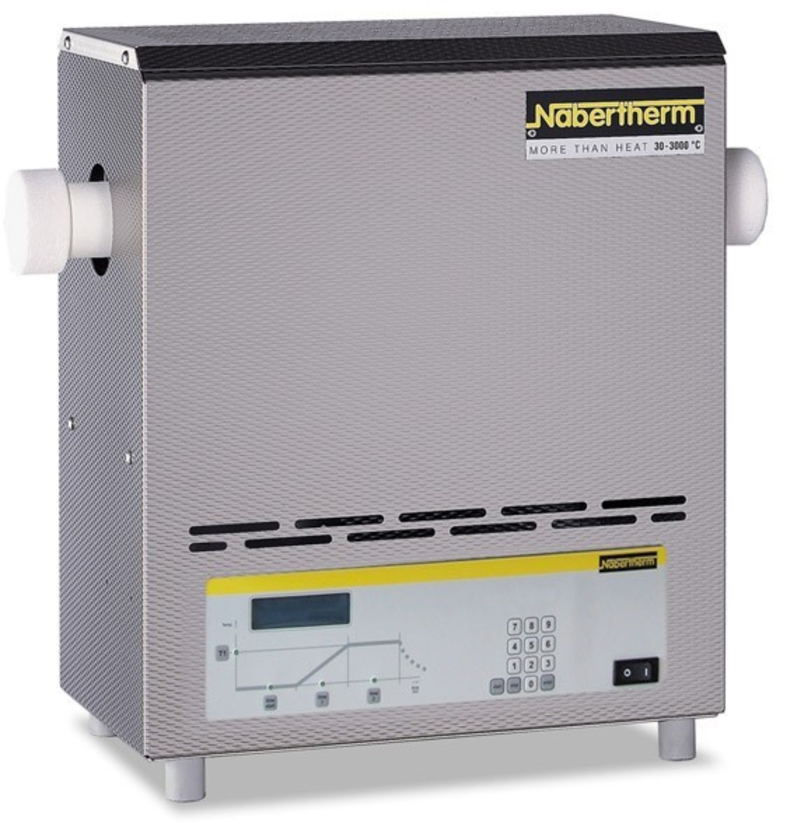 |
Manufacturer: NABERTHERM
(Germany) Model: R50 Price: 4700 € (+ 24% VAT) Characteristics: Compact tabletop tube furnaces with integrated control systems; equipped with a working tube of C 530 ceramic and two fiber plugs, Tmax of 1200C. Housing made of sheets of textured stainless steel, outer tube diameter of 50 mm, heated length tube of 450 mm, type S thermocouple, solid state relays for low noise operation. Program controller B 180, Digital PID-temperature control, one storable program, timer for delayed start, over-temperature protection, auto tune, integrated KW/hr counter, integrated operating hours counter. Gas supply systems for nitrogen and oxygen (one for each) with shutoff valve and flow meter with control valve (volume 50-500 l/hr), 2 plugs of ceramic fiber with protective connections. Oven dimensions: 400x240x490 mm3 (WxDxH), weight of 20 kg. The oven is installed at IMT-Bucharest. |
|
|
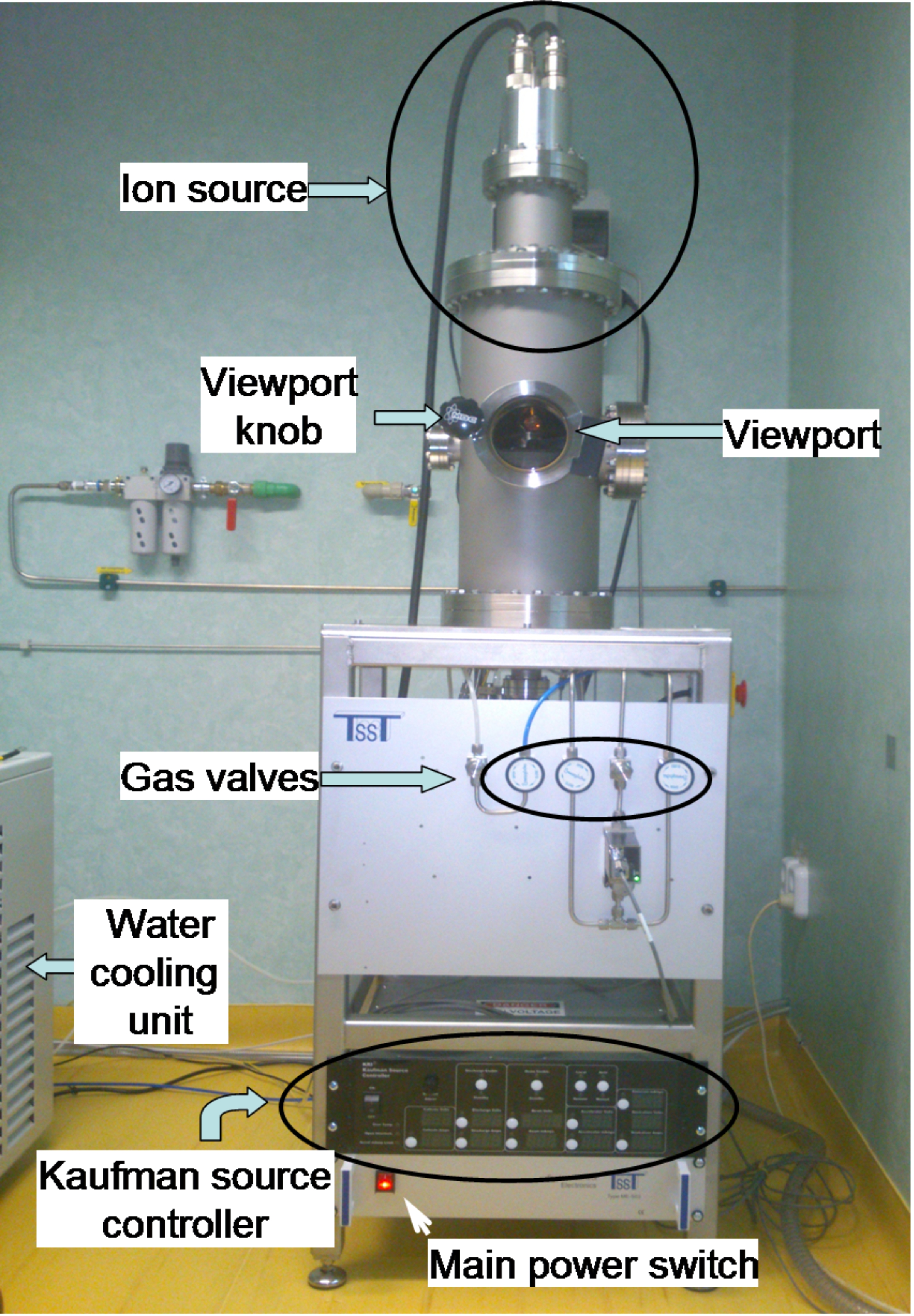 |
Manufacturer: TSST (The Netherlands)
The system uses Ar ions for physical etching (milling) of the material (metals, oxides, polymers) and angles from 0 to 90o (vs. the sample normal), with continuous sample rotation during etching. Characteristics: 1. General characteristics - single chamber system containing an Ar-ion source for etching; - manual loading of the wafers into the process chamber; - sealed, with vacuum (base pressure <5´10-6 mbar) and ventilation; - sample rotation and tilt (0-90o) during etching; - process monitoring software; - it can be used as loadlock in case of a future upgrade (one free port); - safe shut down procedure. |
2. The process chamber
3. Operation
4. Main parameters of the system
4.2. Sample stage of the chamber The system is installed at IMT-Bucharest. |
|
Contact info:
Dr. Victor LecaCenter of Nanotechnology, Laboratory for Molecular Nanotechnology
National Institute for Research and Development in Microtechnologies - IMT Bucharest
Address: 126A, Erou Iancu Nicolae Street R-077190, Voluntari, Ilfov, Romania
Tel: +40-21-269.07.70 (ext. 33)
Fax: +40-21-269.07.72
E-Mail: victor[dot]leca[at]imt[dot]ro.